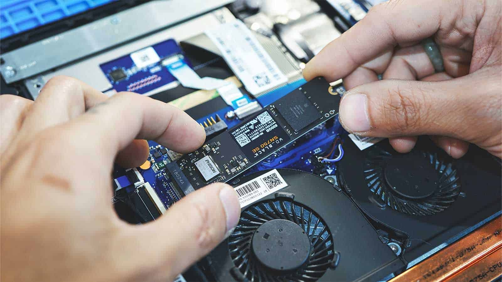

When purchasing technological products, we look at more than one detail, and some of us even go deep into the process. When there are SSDs on the table, there are still many details we can investigate. Endurance time is one of them.
SSD endurance refers to the ability of an SSD to withstand sudden shocks and other environmental conditions and indicates how long it can withstand failures over time. This is just one of the advantages of SSD over HDD.
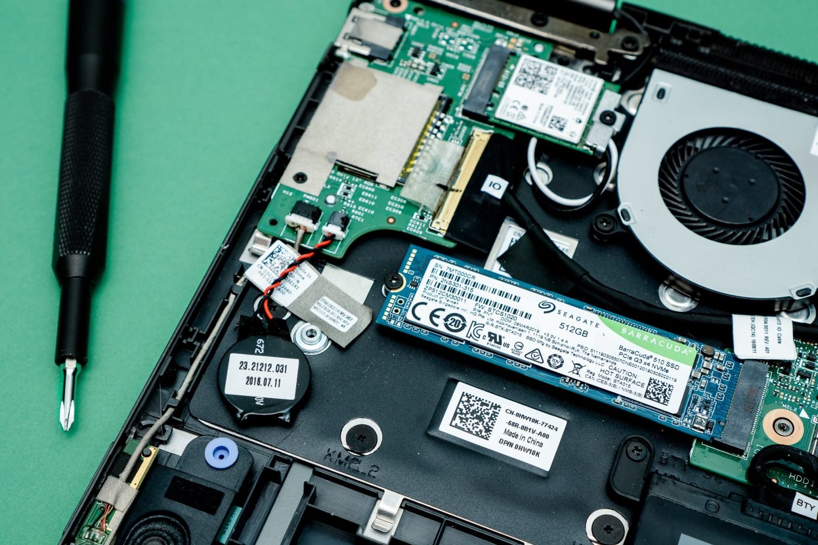
SSDs have gained immense popularity over the last decade and have become the primary storage unit for many users, replacing mechanical hard drives. However, although they are more durable, SSDs have a defect that is often ignored: their lifespan is more limited than hard disks.
We have discussed all the details you need to pay attention to when choosing an SSD in our article above. Now we will look at the durability periods, which are a matter of curiosity for technology enthusiasts.
What Does SSD Endurance Mean?
SSD endurance is calculated by measurements that determine the lifespan of a solid-state drive. These measurements are based on NAND flash memory P/E (P/E) that their cells can achieve before they start to deteriorate Program/Erase) based on the number of cycles.
Memory cells have a limited lifespan because transistors begin to wear out after a certain number of P/E cycles. Beyond this, charging carrying capacities also begin to be affected, and the risk of malfunction and data loss increases.
Essentially, SSD durability depends on the type of cell used; namely SLC, MLC and TLC. In summary, SSDs with more bits per cell have a shorter lifespan:
- SLC NAND Flash: 50000-100000 P/E cycle
- MLC NAND Flash: 3000-10000 P/E cycle
- TLC NAND Flash: 300-1000 P/E cycles
On the other hand, the acumen of the drivers also depends on the storage capacity. More storage space means more memory blocks for data distribution and increased endurance.
SSD endurance is measured in two basic terms: Terabytes Written (TBW) and Data Writes per Day (DWPD). Let’s briefly summarize first:
- TBW: Terabytes written is the total amount of data in terabytes that can be written to an SSD over its lifetime. For example, WD Black SN850 1 TB SSD has 1200 TBW. This means that 1200 terabytes of data can be written securely before any possibility of failure arises.
- DWPD: Data write rate per day, a measure of the amount of data that can be written to the drive each day during the warranty period. A 1 TB drive with a DWPD rating means that one terabyte of data can be written every day during the warranty period.
Think of it this way: SSD is a piece of paper that you use to write on. When you write something on paper or erase it, it wears out after being used for a while. The same goes for SSDs. Solid-state drives with cells have a limited number of times that you can save or delete data in each cell before it completely ceases to function.
Manufacturers also use various values to calculate how long an SSD will last.
P/E Cycle
P/E cycle means program/erase cycle. It reflects the lifespan of the SSD as data is written and deleted to each block in a cycle. This is because the number of P/E cycles the NAND can withstand Showing how long the driver can last.
A limited number of data can be written to the data blocks on the SSD, and once a certain value is reached, it is impossible to write any more data. This is why the P/E cycle is important.
What is Drive Writes Per Day (DWPD)?
Drive Writes Per Day (DWPD) is a measure of how many times you can overwrite the entire size of a drive each day over its lifetime. He sings. For example, let’s assume that your drive is 200 GB and the warranty period is 5 years.
If its DWPD is 1, it means that you can write 200 GB of data into it every day for the next five years. If you multiply that, you get 200 GB per day – 365 days/year – 5 years = 365 TB cumulative writes before you need to replace the product.
If its DWPD was 10 instead of 1, this would mean that you could write 10 – 200 GB = 2 TB (ten times its size) into it every day. This means 3,650 TB = 3.65 PB cumulative writing over 5 years.
What is Terabytes Written (TBW)?
Terabytes Written (TBW) directly measures how much you can cumulatively write to the drive over its lifetime. Essentially, the multiplication we did above is included in the measurement itself.
For example, let’s say your drive is rated at 365 TBW. This means you can write 365 TB of data into it before you need to replace it. If the warranty period is 5 years, this means 365 TB (5 years 365 days/year) = 200 GB of data per day. If your drive is 200 GB in size, the result is equivalent to 1 DWPD er. On the other hand, if your drive is rated for 3.65 PBW = 3,650 TBW, this corresponds to 2 TB writes per day or 10 DWPD.
As you can see, if you know the size and warranty period of the drive, you can calculate the DWPD and TBW values with some simple multiplication or division. The two measurements are very similar indeed.
TWB vs. DWPD: What’s the Difference?
The only real difference is that DWPD depends on the size of the drive while TBW does not. Take, for example, an SSD that can handle 1,000 TB of writes over its 5-year lifetime.
Let’s assume the SSD is 200 GB:
1,000 TB ÷ (5 years × 365 days/year × 200 GB) = 2.74 DWPD
Now let’s assume the SSD is 400 GB:
1,000 TB (5 years – 365 days/year – 400 GB) = 1.37 DWPD
The resulting DWPD is different. What does it mean?
The larger 400 GB drive performs the same cumulative writes over its lifetime as the smaller 200 GB drive. It can improve. This is very clear when looking at TBW and both drivers are rated at 1,000 TBW. However, looking at the DWPD reveals that it only has half as much durability as the larger driver.
On the other hand, since the 400 GB drive is larger, it provides more storage with more workload. As a matter of fact, we can say that 1,000 TBW is spread more thinly and has only half the durability. By this logic it is better to use DWPD.
What is Mean Time Between Failures (MTBF)?
MTBF, which stands for Mean Time Between Failures, is a statistical measure that represents the average time a component or system is expected to operate before experiencing failure. It is usually expressed in hours and is used to estimate the overall durability and longevity of hardware components such as hard drives, power supplies, and other critical parts of a computer system. for one It is used as a criterion of reliability.
A higher MTBF value indicates that the hardware is more reliable and durable. In other words, the component is less likely to fail within the specified time period. Let us remind you that MTBF is an estimate based on statistical data and models. That means a particular component is not guaranteed to last exactly as long as its MTBF value.
How to Calculate MTBF?
The calculation formula is as follows:
MTBF = Total Operating Time / Number of Failures
You can follow the four steps below:
- Determine the period for which you want to calculate MTBF. This can be a specific period of time, such as a month, a year, or the entire lifecycle of the component or system.
- Record the total operating time of the component or system over the selected period. The uptime must be measured in the same units as the MTBF you want to calculate (e.g. hours).
- Count the number of failures that occur during the same period.
- Use the formula mentioned above to calculate MTBF by dividing the total uptime by the number of failures.
For example, let’s say you want to calculate the MTBF of a hard drive over the course of a year. During this year, the hard drive operated for 8,760 hours and experienced 2 failures. Therefore, the MTBF of this hard drive over a year is 4,380 hours per failure. This means that on average the hard drive operated for approximately 4,380 hours before experiencing a failure during that year.
How Important Are SSD Endurance Values?
To be honest, these values are not very important for standard users who use their computers routinely. How much data do we write in a day? To better understand the situation, see “How Long Will It Last?” on Technopat Social YouTube channel. You can watch labeled SSD videos.
However, the quality, lifespan and durability values of SSDs are very important for people/institutions that constantly work with storage drives.
How to Increase SSD Durability and Lifespan?
- TRIM: TRIM helps an SSD maintain its performance over time by optimizing data storage capacity, which extends its lifespan.
- Temperatures: Avoid extreme temperatures. Operating your SSD beyond temperature specifications can result in degraded performance and premature failure, so always keep temperatures within the manufacturer’s specifications. Try to keep it within the shading range.
- No need for merge feature: Disable SSD defragmentation feature. SSDs do not need defragmentation.
- ECC: Error correction code (ECC) corrects random bit errors and reduces wear. The use of ECC extends the usable life of flash cells.
- SSD software: It is useful to use tools developed by manufacturers to manage SSD, follow detailed information and use extra features.
How to Check TBW Value?
If you are curious about the TBW value of your current SSD, follow the method below:
- Download the CrystalDiskInfo utility from here Download and install it on your computer.
- Open the software and wait for it to detect all your drives.
- Once installed, find the SSD you want to check in the top line and click on it.
- At the top right, find the box that says “Total Host Writes.” You can hover your mouse cursor over the number to see the TB value.
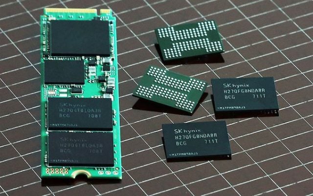
NAND Memory Types
“NAND†is a very inclusive expression. In this context, there are many different designs and subclasses.
What is SLC (Single Level Cell)?
SLC chips provide the most stable response in read and write situations and remain more durable over multiple read/write cycles. A lifespan of around 90,000 to 100,000 read/write cycles is expected for these chips. It has achieved success in the business world due to its useful life. It is unlikely that you will see this type of NAND chip in any home computer due to its high cost and low storage capacity.
Advantages:
- It is long lasting and offers more cycle opportunities.
- More stable with fewer read/write errors
- Ability to operate at very wide temperature ranges
Disadvantages:
- Being the most expensive NAND chip on the market
- Suitable for low capacity solutions
It is recommended for use in areas that require heavy read/write power, such as servers.
What is MLC (Multi Level Cell)?
Since MLC chips are lower cost than SLC, they are used by many manufacturers in products for home users. It has a lifespan of approximately 10,000 read/write cycles per cell.
Advantages:
- More cost-effective for home users
- More stable than TLC chips
Disadvantages:
- It is not as stable and performant as the SLCs used in the business world.
Recommended for gamers and home users.
What is TLC (Triple Level Cell)?
These chips, which store 3 bits of data per cell, are among the cheapest to produce. Its biggest disadvantage is that it does not meet business use standards and is only suitable for daily use. The read/write cycle lifetime per cell is expected to be between 3,000 and 5,000.
Advantages:
- Being the cheapest NAND chip
Disadvantages:
- Compared to MLC NAND memories, the cells have a shorter read/write cycle life. That’s why these memories are only suitable for daily use.
It is ideal for devices such as computers and tablets that operate at low usage intensity.
What is QLC?
Quad-level cell (QLC) flash memory, or QLC SSD (solid-state drive), is a capacity-optimized NAND memory technology that offers a cost per terabyte that matches or exceeds hard disk drives (HDDs). As the name suggests, QLC SSDs offer NVMe performance at higher capacities by storing four bits per cell.
HLC and OLC Started to Be Discussed
Kioxia, formerly known as Toshiba Memory, was the first manufacturer to make statements about 5-bit per cell PLC (penta-level cell) 3D NAND memories in 2019. Company engineers have now confirmed that they are working on 6 bits per cell (HLC) 3D NAND memories. They even believe that chips with 8 bits per cell (OLC) are possible.
To store more than one bit per cell, NAND memory must maintain more than one voltage level in that cell. For example, MLC uses four voltage levels per cell, while TLC uses eight. There are 16 voltage levels in QLC and 32 voltage levels in PLC. In order to store six bits per cell (HLC), it is necessary to have 64 voltage levels.
As a matter of fact, developing 3D NAND chips with such cells is very difficult and many difficulties must be overcome. On the other hand, finding the right materials that can maintain voltage, keep temperatures under control and many other studies are required.
To demonstrate the possibilities of HLC memory, Kioxia’s engineers took one of the existing 3D NAND chips and added fluid to prevent degradation caused by rewrite cycles. ± used nitrogen. Ultimately, they managed to write and read six bits of data from a cell and operate it reliably for 100 minutes.