
The battle of the giants continues. The second half of 2024 will host important innovations in the CPU world. While AMD transitioned to hybrid architecture with Ryzen AI 300 mobile processors, it also made serious breakthroughs in the field of artificial intelligence. Intel responded to its rival by announcing the Lunar Lake architecture during the Intel Tech Tour 2024. gave. The new architecture will be used first in Core Ultra 200V mobile processors.
In fact, Intel’s rival is not only AMD, but also Apple and Qualcomm. Being aware of everything, the company has decided to make radical changes. With Lunar Lake, the design of the processors changes from a to z. By the way, let’s make a small note: Lunar Lake architecture is aimed at mobile platforms and laptops. However, we will probably see most of the basic design changes on the desktop Arrow Lake side as well. In other words, desktop Intel CPUs that will be released soon will also come with serious innovations.
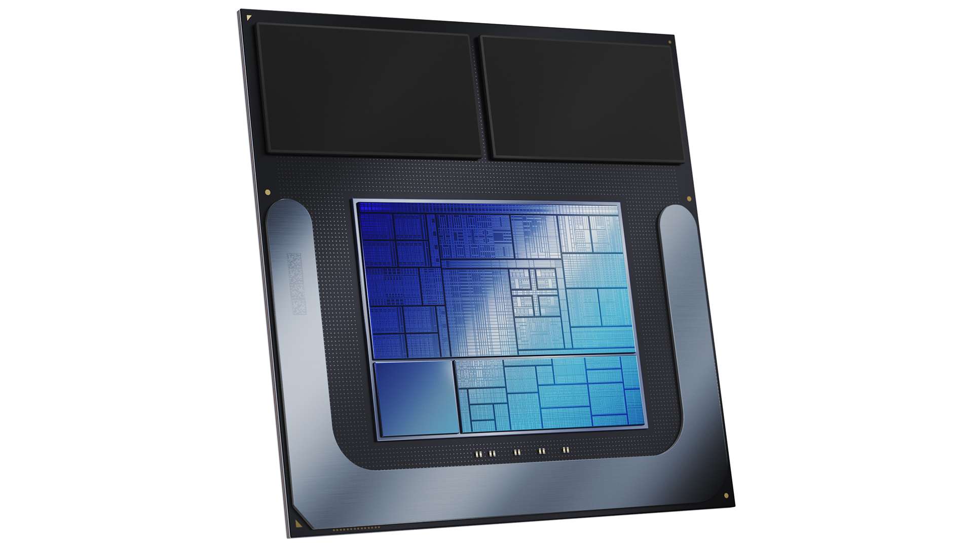
The architecture, the details of which are exhibited, is supported by advanced connection and packaging technologies, including memory-on-package (MoP) technologies. Intel Core Ultra 200V Lunar Lake is no longer a CPU, it has become a complete SoC (system on a chip) design. There will also be no system memory in the design. The new processors come with LPDDR5X memory in capacities up to 32 GB.
Intel has designed its new designs to appeal to both general use and new generation AI PC platforms such as Microsoft Copilot+. Chips that do not compromise on performance are both highly efficient and very successful in artificial intelligence workloads. To summarize, Lunar Lake provides high core performance, breakthrough x86 power efficiency, high artificial intelligence calculation performance and advanced graphics performance.
The Core Ultra 200V series will compete with series such as Apple M3, Qualcomm Snapdragon X Elite and Ryzen AI 300. Initially, at least two models with Lunar Lake architecture will be released, but the final features of these models were not shared in the presentation. Focusing on artificial intelligence, the technology giant plans to ship 40 million artificial intelligence-enabled processors by the end of the year, and Lunar Lake chips are already in the company’s factories. The chips will reach shipping systems in the 3rd quarter of 2024.
What Changed with Lunar Lake Architecture?
As you know, Intel has been producing hybrid processors with different core types for years. The idea behind the hybrid was to develop CPU cores that offer different power consumption values so that the processor can better respond to software processing loads. While the performance cores we call P-Core deal with intense and heavy workloads, the efficiency cores we call E-Core handle low priority and light workloads. It was designed to. The company also worked on a hardware solution called Thread Director so that the CPU can communicate better with the operating system. Thread Director is a hardware component developed to ensure that the correct cores run depending on the workload.
With Lunar Lake, Intel has updated the microarchitecture of all four key components of the SoC: CPU processing complex two next-generation CPU cores offers; integrated graphics (iGPU) comes with a new graphics architecture; and the NPU has been both updated and strengthened to meet Copilot+ AI PC requirements. In addition to these, there are many updates that Intel has made on silicon. A switch was made to on-package memory design, and this was a radical decision. Just like chips like the Apple M3 and Qualcomm Snapdragon X Elite.
Every component of the Lunar Lake architecture has been optimized for a refined blend of power and performance that Intel says will redefine what we expect from x86 PCs. The biggest improvement is undoubtedly in the efficiency cores. With the transition to Skymont architecture, IPC gains of 38% and 68% were experienced. Lion Cove architecture brought a 14% IPC gain to the performance cores. Graphics provided a 50% improvement in iGPU performance with the new Xe2 integrated graphics engine.
It is no longer possible without opening a separate parenthesis for artificial intelligence. Mobile processors will be offered with the new neural processing unit (NPU) offering 48 TOPS performance for artificial intelligence workloads. Thus, the 40 TOPS NPU requirement that Microsoft required for the new generation artificial intelligence computers was easily met. If you remember, AMD was offering 50 TOPS NPU performance with its XDNA 2 architecture and Ryzen AI 300 series. Intel, on the other hand, is almost on par with its rival if only NPU is taken into account. However, the Lunar Lake platform has much more AI performance: When we take into account the CPU and iGPU, a total performance of 120 TOPS is promised.
Lunar Lake mobile chips use an entirely new design methodology that focuses on ensuring power efficiency as a top priority, and this underlying architecture serves as the building block for future products from Intel such as Arrow Lake and Panther Lake. will be adopted. This new design focus will be key for the company to compete with strong rivals from AMD, Apple and Qualcomm in the laptop market.
Surprisingly, Intel turned to TSMC for the computing die that houses the CPU, GPU and NPU, using 3nm (N3B) process technologies. They also used TSMC’s 6nm (N6) technology for the controller platform die, which includes external I/O interfaces. The only silicon on the chip produced by Intel is the passive 22FFL Foveros base system chip, which facilitates communication between the chip dies and the main system.
Intel says that when they started designing the chips, TSMC solutions were the most options available. What they mean is that there was no other option. The blue giant had a goal of regaining its leadership on the foundry side through five separate process technologies within four years.
The election made by TSMC once again proved the delay in the targets. However, Intel designed the architectures to be easily ported to other processing processes. As a matter of fact, the company will be able to use the same architectures in its own foundries for its future products. Lunar Lake’s new microarchitectures pave the way for the company’s soon-to-be-announced Arrow Lake processors for desktops and even the Xeon 6 series. Now let’s move on to the details.
The models in the Core Ultra 200V series have not been announced yet. The top-end processor will come with 4 P-Core and 4 E-Core. The chip consists of two logic dies, a TSMC N3B compute die, an N6 platform controller die, and the 22FFL base Foveros die. On top of all this, there is also a non-functional filler silicone piece.
Intel builds two LPDDR5X-8500 memory stacks in 16GB or 32GB configurations to reduce PCB area along with latency and reduce memory PHY power consumption by up to 40% Direct to chip package placing it. The memory will communicate over four 16-bit channels and deliver up to 8.5 GT/s per chip.
The computing unit includes the CPU performance and efficiency cores, the Xe2 GPU and the artificial intelligence chip called NPU 4.0. A new 8 MB ‘side cache’ that can be shared between all various compute units has also been integrated to increase hit rates and reduce data movement, thus saving power. Â However, this cache does not technically meet the definition of L4 cache because it is shared among all volumes.
Intel has also moved the power distribution subsystem from chip to board and spread four PMICs across the motherboard to provide multiple power rails and greater control. Overall, Intel claims a 40% reduction in SoC power compared to Meteor Lake.
P-Core: Lion Cove Performance Cores
Lunar Lake’s performance cores bring to the table an average gain of 14% in IPC (Instructions Per Cycle). However, Intel has implemented Hyper-Threading (multi-threading) and built the cores into a hybrid architecture by removing all the logic blocks that provide this performance-enhancing feature. While optimizing it took an unexpected turn.
Intel’s engineers concluded that Hyper-Threading technology, which increases IPC by ~30% in thread-intensive workloads, is not that important in hybrid design. Threads were often first scheduled into P-Cores before taking advantage of the extra threads in the cores, then the additional threads were assigned to E -It was directed to the Cores. After the E cores reached saturation, additional threads began to be scheduled to the extra threads in the P-Core.
Removing the special mechanisms and extra security features required for Hyper-Threading makes the kernel leaner, resulting in a 15% increase in performance efficiency, a 10% increase in performance per domain, and a 10% increase in performance per domain. Provided a 30% increase in performance per power. This was much more effective than just disabling Hyper-Threading while leaving the control circuitry present. The new approach also preserves die space for other components such as more E-Core or GPU cores.
However, Intel is not leaving Hyper-Threading aside completely; This technology will only be used in some P-Core designs. The company has designed two versions of the Lion Cove core, one with hyperthreading and the other without hyperthreading. Thus, the threaded Lion Cove core can be used in other applications, as we see in the upcoming Xeon 6 processors.
Lion Cove also includes predefined static settings for a variety of operating conditions, such as assigning specific points on the voltage/frequency curve for different thermal and power thresholds. a transition also points out. An AI auto-tuning controller is now used to dynamically adapt more intelligently. Intel’s clock frequencies were also previously only adjustable in 100 MHz increments. It can now be tuned in 16.67 MHz increments to provide finer-grained frequency and power control. The tech giant attributes this to single-digit percentage increases in power efficiency or performance in some scenarios, and every bit counts in an efficiency-focused architecture.
Intel says it has expanded the prediction block by 8 times over the previous architecture while maintaining accuracy. In addition, the request bandwidth from the instruction cache to the L2 has been tripled and the instruction fetch bandwidth has been increased from 64 to 128 bytes per second. Additionally, the code is output. The decoding bandwidth has been increased from 6 to 8 instructions per cycle, while the micro-op cache has been increased along with the read bandwidth. The micro-op queue also increased from 144 entries to 192 entries.
Previous P-Core architectures had a single scheduler to distribute instructions among execution ports, but the design introduced hardware overhead and scalability issues . Wanting to address these issues, Intel expanded its unconventional engine to integer and vector fields with independent renamers and timers to increase flexibility. He allocated it to . A number of improvements have also been made to the retirement, command window and execution ports, as well as the integer and vector execution pipelines.
The memory subsystem has a new L0 cache level. Engineers completely redesigned the data cache to add a 192KB layer between the existing L1 and L2 caches. Ultimately, the L1 type cache was renamed L0. With the changes in cache design, the average load-usage time was reduced, which increased the IPC, and the L2 cache capacity was increased without sacrificing latency due to the increased capacity. As a result, the L2 cache will be able to go up to 2.5 MB on Lunar Lake and 3 MB on Arrow Lake. Both architectures will use Lion Cove architecture P-Cores.
The rope manufacturer has also moved from using proprietary design tools to industry standard tools optimized for its use. Intel’s legacy architectures were designed with tens of thousands of cells of “Fubs” (functional blocks) made up of hand-drawn circuits. Now large, synthesized sections consisting of hundreds of thousands or even millions of cells can be used. Removing artificial boundaries reduces design time and More efficient use of space while improving the process It provides this.
This also enables more configuration options to be added to the design to more quickly come up with customized SoC-specific designs. ladi. Intel says the change in process allows for greater customization between the cores used for Lunar Lake and Arrow Lake. Thanks to this design methodology, 99% of the design can also be transferred to other process technologies, in other words, it can be adapted. This means that Intel will be able to use its own foundries instead of TSMC’s technologies in the future.
As a result of the changes, a 14% increase in IPC with a fixed clock speed was achieved compared to the previous generation Redwood Cove architecture used in Meteor Lake. The CPU manufacturer also points to overall performance improvements ranging from 10% to 18% over Meteor Lake, depending on the chip’s operating power. Power/performance improvements are based on projections/estimates, so Intel has given itself a +/- 10% margin of error for measurements in the ‘performance on power’ table.
E-Core: Skymont Efficiency Cores
We talked about numerous changes to the Lion Cove core architecture. But Skymont appears to have made an even bigger improvement over the previous generation, with a 38% IPC improvement on integer workloads and a 68% IPC gain on floating point jobs. Up to 2x increase in single-thread performance and up to 4x increase in multi-thread workloads compared to low-profile E-Cores in Meteor Lake chips ksek performance was achieved. Intel also doubled throughput on vectorized AVX and VNNI workloads.
Skymont became the third E-Core core design designed for x86 Intel hybrid processors, following Gracemont at Alder Lake and Crestmont at Meteor Lake. The previous Meteor Lake design included 2 LP E-Cores built into the SoC die and P-Cores into the CPU unit for ultra-low power workloads. 4 additions added We have seen E-Core. By changing the process with Lunar Lake, Intel is working to address both low-power E-Core and high-power E-Core roles with an expanded dynamic range. Uses a single quad-core cluster in the compute unit .
The blue team optimized the branch prediction engine by adding a parallel fetch of 96 instruction bytes to feed the decoding engine. Increased the width level in decoding clusters from 6 (2×3, Crestmont) to 9 (3×3, Skymont). So any core in the new design will be able to decode nine instructions per clock. Skymont also now uses nanocode to enable parallel microcode generation so that three decoding clusters run in parallel more often. . Micro-op capacity has also been increased from 64 to 96 inputs to add more buffering between the front-end and back-end.
However, in order to free up resources as quickly as possible after pauses, Crestmont’s 8-wide retire operation was doubled to 16. Thus, power and space efficiency increased. “The out of order window” is 60% larger than the previous generation. These terms are quite foreign, but let’s note that the architecture provides larger register files, deeper reservation stations, and deeper load and storage buffering. Parallelism, eight ALUs, three jump ports, and Increased by using 26 transmit ports, including three upload/translation support.
With Skymont, Intel aims to achieve a 2-fold improvement in vector performance, increasing from two 128-bit FP and SIMD vector lines to four. Latency in the vector engine has been reduced and floating point rounding support has also been added.
The previous clusters containing efficiency cores had 2 MB of L2 cache shared, which has doubled to 4 MB. Moreover, the L1 to L1 transfer bandwidth has also been improved.
The 38% and 68% improvement in single-threaded integer and floating point performance is truly impressive. However, this comparison was made specifically with the low power (LP) E-Cores in the Meteor Lake SoC; Not with the standard E-Cores located with the P-Cores in the CPU unit. The company says that there may be a large margin of error of +/- 10% in its comparisons.
Skymont’s power and single-threaded performance curve are greatly improved over Crestmont, but the benchmarks are the same It was made against LP type nuclei as follows. Compared to Crestmont’s peak performance, Skymont consumes one-third the power to deliver the same level of performance. However, 1.7 times more performance can be achieved at the same power level. Overall, Skymont’s peak single-threaded performance is twice that of Crestmont LP E-cores.
Skymont’s 4-core cluster is again not compared to the similar 4-core cluster, but instead Meteor Lake’s dual-core low power cluster ¼ Encountered the E-Core cluster ±broken. That’s why we talked about to large percentages Don’t worry too much.
Intel also made comparisons between Skymont and Raptor Lake’s performance cores that use the Raptor Cove architecture. So, interestingly, performance and efficiency cores were compared. At this point, it is stated that Skymont has a 2% advantage in integer and floating point performance. However, it has been said that there may still be a high margin of error.
A Leap in Graphics Performance: Lunar Lake Xe2 GPU
The new Xe2 integrated GPU delivers up to 1.5x more graphics performance and up to 67 TOPS of AI performance compared to Meteor Lake’s Arc Graphics. Intel has also simplified the naming of the GPU architecture: all configurations will only have the name Xe2, as opposed to the Xe-LP, Xe-HP and Xe-HPG suffixes used in the previous generation Xe architecture.
Intel’s Xe2 architecture will be used not only in Lunar Lake processors, but also in the upcoming Battlemage gaming GPUs. Of course, the external and internal GPU will not be the same. While the underlying architecture is the same, Lunar Lake will use lower power transistors while Battlemage will use faster transistors to maximize performance. We’d like to make performance predictions for upcoming Intel graphics cards, but it’s not easy to make a prediction since everything will be different. External graphics cards are different in everything from design to memory.
The Xe2 GPU architecture includes Intel’s second-generation Xe cores, larger deeper caches Contains. The GPU is dedicated to second-generation Xe cores and render slices, as well as fixed-function graphics hardware for tasks like geometry rendering, texture sampling, and rasterization. These units depend on a large cache and memory structure, as well as I/O hardware that varies depending on the application. The design is modular in nature, meaning it can be easily scaled to use more or fewer units.
The second-generation Xe core will be able to perform eight 512-bit multiplies per clock on XVE vector engines and eight 2048-bit vectors per clock on XMX engines. Intel has also expanded the SIMD engine from 8 lanes wide to 16 lanes wide, a more common arrangement that will improve compatibility. Additionally, we should point out that the kernel uses 192 KB of shared L1 cache.
The second generation vector engine supports INT2, INT4, INT8, FP16 and BF16 commands for artificial intelligence operations. You can see the calculations showing high TOPS values in the slide images provided by Intel.
The graphics processing unit has also received many large and small improvements; 3x vertex fetch efficiency increase by changing vertex distribution along the pipeline, improving mesh shading performance through vertex reuse double Like removal, new support for out-of-order sampling, and twice the throughput for sampling without filtering. The company also states that beam tracking performance has increased thanks to the reorganized pipeline in the new Xe Ray Tracking Unit (RTU).
Artificial Intelligence: NPU 4.0
NPU, the central component of the artificial intelligence strategy, increased to 48 TOPS performance level, as we mentioned before. However, the NPU is primarily designed for low-intensity tasks, so it can save a tremendous amount of battery power. The GPU will step in for more demanding workloads with 67 TOPS of performance. The CPU, on the other hand, will be able to contribute to artificial intelligence workloads with smaller amounts such as 5 TOPS. Thus, a Lunar Lake SoC will be able to offer a total of 120 TOPS artificial intelligence performance.
The big story here is that the NPU 4 powering Lunar Lake has 4 times the AI inference performance of the NPU 3 found in Meteor Lake. AI inference performance jumped from 12 TOPS in Meteor Lake to 48 TOPS in Lunar Lake. This amount meets and easily exceeds the 40 TOPS requirement set by Microsoft to speed up Copilot+ local sessions and qualify for Copilot+ AI PC certification .
This linear scaling in AI inference performance is not only due to architectural improvements (trying to reduce the power footprint of the NPU), but also NCE (neural computation engine) It is also due to their numbers. The amount of NCE, which was 2 in the Meteor Lake architecture, was increased to 6 with Lunar Lake. RAM, DMA bandwidth and L2 cache also improved proportionally.
The AI unit supports matrix multiplication and convolution (MAC) array, INT8 and FP16 data types with 2048 MAC/cycle INT8 or 1024 MAC/cycle FP16. Intel claims a twofold increase in performance/Watt over the NPU 3, thanks to improvements in activation functions, data conversion, upgrades to SHAVE DSP, and a twofold increase in bandwidth of the DMA engine It does. The raw vector performance of NPU 4 is now 12 times that of NPU 3, 4 times that of AI TOPS, and 2 times the bandwidth to tissue of NPU.
Link
Built on the TSMC 6nm process, the platform I/O unit carries all SoC interfaces and platform connections. Interestingly, the processor’s memory controllers are located in the Compute section, which includes the CPU cores, iGPU, and NPU. This memory controller only supports LPDDR5X, because only memory integrated on the package can be used.
Including an integrated WLAN controller with I/O chip Wi-Fi 7 + Bluetooth 5.4, support for 5.8 Gbps WLAN bandwidth and support for up to three 40 Gbps Thunderbolt 4 ports It brings together many new generation components. The PCI-Express root complex is also located here. Lunar Lake offers only 8 PCIe lanes; Four of them are Gen 5 and the other four are Gen 4.
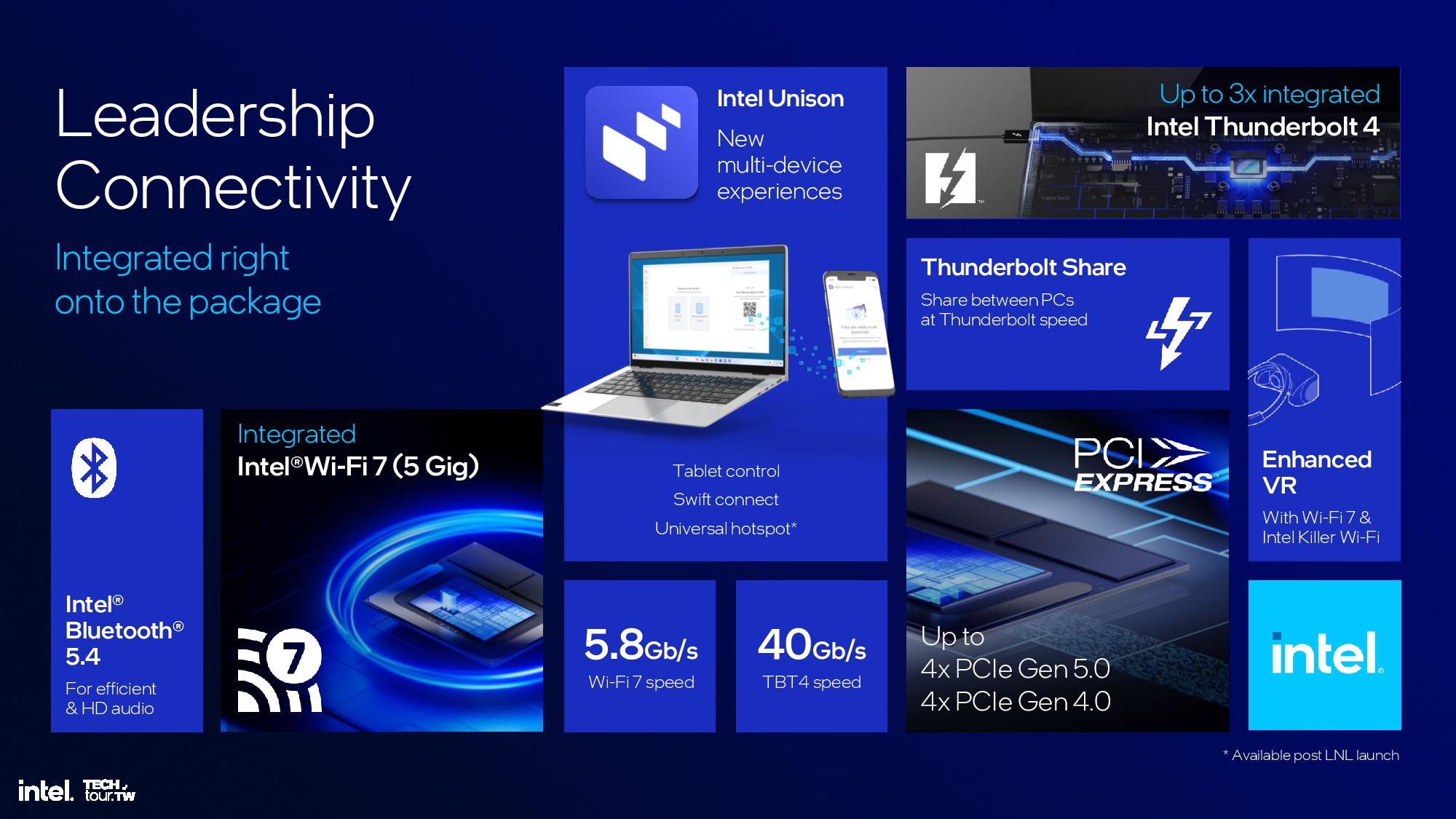
The idea behind just 8 PCIe lanes stems from the type of device the Core Ultra 200V family targets. The new generation chips will be used in thin and light laptops, moreover, there will be no external GPU. Four Gen5 lanes will drive next-generation PCIe 5.0 NVMe SSDs, while the other four Gen4 lanes will be left for platform connections.
Lunar Lake supports USB 2.0 connectivity along with 5 Gbps and 10 Gbps USB 3.2, as well as up to 3 Thunderbolt 4 40 Gbps ports. Again, there aren’t many ports and you won’t need them on this type of device. An expansion slot or a Thunderbolt-based eGPU can be used if necessary.
Thread Director Enhancements
To summarize, the hardware-based Thread Director technology, which enables the operating system to communicate better with the cores inside the processor, has also gained various improvements. Power consumption and performance optimizations were made. Core selection has been improved along with timings.
To briefly describe Lunar Lake, we can say that it is a major architectural upgrade from Intel in the field of mobile SoC, directly compared to Meteor Lake. The engineers of the blue team have left almost no place untouched in the architecture. There is a change in every area, from performance cores to efficiency cores, from artificial intelligence workloads to integrated graphics performance and connections.
| Alder/Raptor Lake | Meteor Lacquer |
lunar Lacquer |
Arrow Lacquer |
panther Lacquer |
|
| P-Core Architecture | Golden Cove/ Raptor Cove |
Redwood Cove | Lion Cove | Lion Cove | Cougar Cove? |
| E-Core Architecture | gracemont | crestmont | Skymont | Crestmont? | Darkmont? |
| GPU Architecture | Xe-LP | Xe-LPG | Xe2 | Xe2? | ? |
| NPU Architecture | – | NPU 3720 | NPU 4 | ? | ? |
| Active Chip Sections | 1 (Monolithic) | 4 | 2 | 4? | ? |
| Production Technology | Intel 7 | Intel 4 + TSMC N6 + TSMC N5 | TSMC N3B + TSMC N6 | Intel 20A + other | Intel 18A |
| segment | Mobile + Desktop | mobile | Low Power Mobile | High Performance Mobile + Desktop | Mobile? |
| Release Date | 4.Ç-2021 | 4.Ç-2023 | 3.Ç-2024 | 4.Ç-2024 | 2025 |