
If you have used or are currently using an NVIDIA branded graphics card, CUDA Cores are at your disposal. So what is this CUDA that we encounter every day?
The processing units found in the graphics chips developed by the green team are called “CUDA Core”. This term, which stands for “Compute Unified Device Architecture”, firstly refers to parallel computing capability and It began to be used to define APIs that allow us to access NVIDIA’s instruction set.
It is safe to say that the frequently mentioned CUDA cores are the backbone of NVIDIA signed GPUs. First introduced in 2006, CUDA has since become an essential part of high-performance computing. Graphics processors have become more powerful day by day and have begun to take on more and more workload that is destined for CPUs. Parallel processing is very important, especially in tasks such as video processing and deep learning. GPUs are perfect for this job.
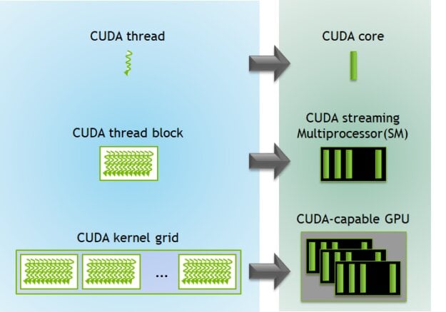
 To take advantage of the parallel processing capabilities of a GPU, software developers need to write code that can break a task into smaller pieces to be worked on simultaneously. This coding is known as “parallel code” and can be run using threads on the GPU.
Now let’s talk about the structure and differences of CUDA Kernels. First, let’s talk about GPUs in general.
Structure of GPUs
Let us state from the beginning that every architecture has its own unique design. On the technical pages you will see many details such as core numbers, ray tracing units, computing units and memory size. However, many things vary from company to company and even from architecture to architecture. Let’s start like this: When comparing between two different graphics cards, you cannot make a decision by looking at the number of cores.
Companies such as AMD, Intel and NVIDIA take completely different approaches when designing graphics chips. Additionally, there may be changes in architectures depending on the target audience and product class. For example, AMD uses Navi 31 GPU silicon for its high-end graphics cards. This graphics chip was used in the Radeon RX 7900 series, which is preferred by those who want high-end performance.
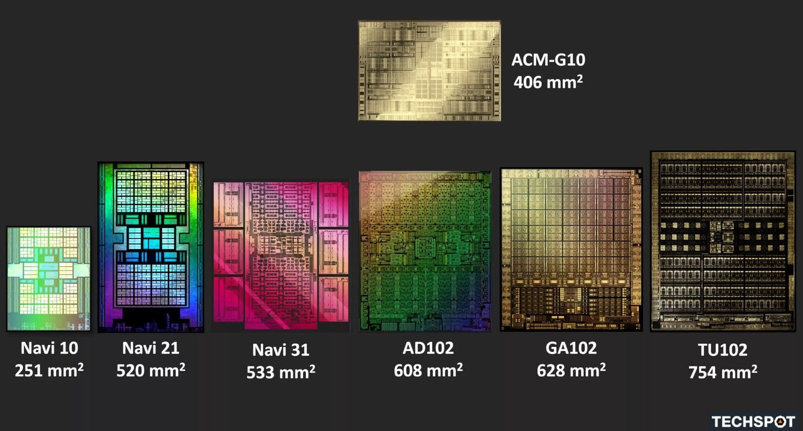
Competitor Greens designed the AD102 graphics chip for the RTX 4090 series, which is aimed at the premium market. These cards do not currently have a rival because RX 7900 graphics cards can compete with the RTX 4080 series. Intel’s current largest and most powerful GPU is called ACM-G10. However, the blue team is still new to the market; They can compete with products such as RTX 3060/RX 6600.
Additionally, just as NVIDIA designs CUDA cores, AMD engineers develop cores called Stream Processor (SM) and Intel engineers develop cores called Xe Core.
What is CUDA Kernel?
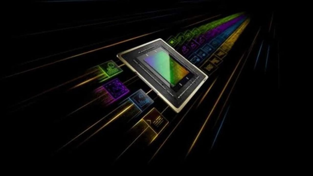
CUDA Cores, in simplest terms, are parallel processing units found in NVIDIA GPUs. These cores allow GPUs to contribute to rendering along with rendering applications by performing calculations and executing tasks in parallel with the CPU. Moreover, CUDA Kernels are designed specifically for CUDA programming. This allows developers to use the power of GPUs for general-purpose computing tasks beyond just rendering.
CUDA cores can work together in harmony to process data simultaneously, making calculations much faster compared to traditional CPU processing. Additionally, each CUDA core has the ability to execute multiple instructions simultaneously. In summary, we can say that GPUs are quite efficient for parallel workloads.
Let’s take an example to understand the working of CUDA kernels. Think of the processor as a water tank. If you want to empty the tank, you need to use pipes. If you connect more pipes, you can naturally empty the tank faster. NVIDIA’s cores act like these pipes to the processor. With more CUDA cores, we can perform the operation faster.
Modern NVIDIA GPUs, as you know, come with three different types of processing cores:
- CUDA cores
- Tensor cores
- Ray Tracing Kernels
Each core is specially designed for different purposes. If you are interested, you can find information about Tensor and Ray Tracing Kernels in our article below. We will now continue with CUDA Cores, which are the most basic of NVIDIA cards.
The green team builds all their architectures on CUDA Cores, including Tesla, Fermi, Kepler, Maxwell, Pascal, Volta, Turing, Ampere and Ada Lovelace. However, the same cannot be said for Tensor Cores or Ray-Tracing Cores.
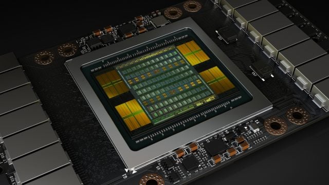
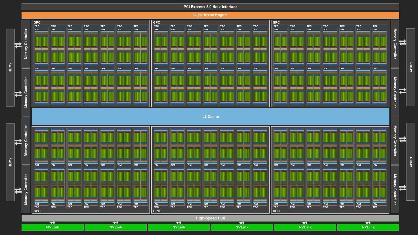
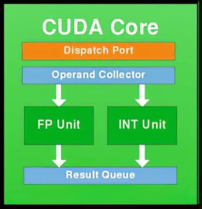
The first Fermi GPUs were designed with SMs (Streaming Multiprocessors), each with 32 cores (CUDA). Up to 512 CUDA Cores could be interoperated with a maximum of 16 SMs. Additionally, these GPUs supported a maximum of 6 GB GDDR5 memory. Here is a block diagram showing the structure of a Fermi CUDA Core. Each CUDA core had a floating point unit and an integer unit.
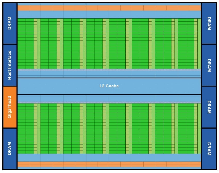
The next figure shows the block diagram of Fermi GPUs. So, an overview of the GPU.
As you know, companies are constantly working to improve the performance and efficiency of GPUs. In architecture-based developments, sometimes the number of cores increases, and sometimes improvements are made on the efficiency side along with performance improvements. For example, with the Kepler architecture, the number of CUDA cores was tripled. The Kepler architecture supported 1536 CUDA Cores and was based on 28nm fabrication technology.
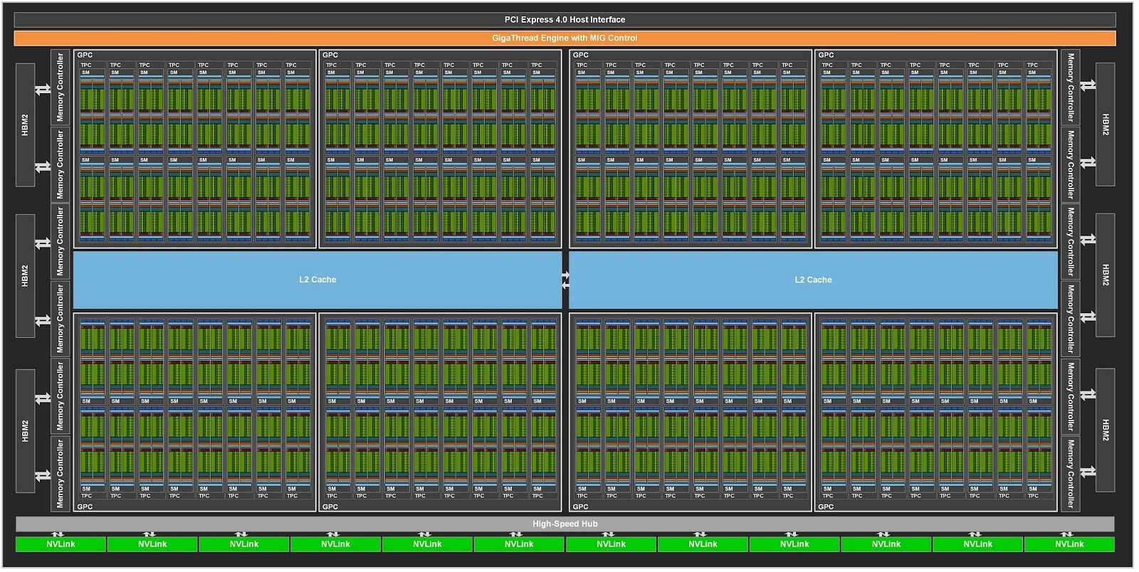
After that, NVIDIA continued to add more CUDA Cores with each new generation. This is what the block diagram of NVIDIA Quadro GP100 looked like. This GPU was part of the Pascal architecture released by NVIDIA in 2016.
Both the Maxwell and Pascal architectures had 128 CUDA cores per stream multiprocessor (SM). In the Maxwell architecture, the integer unit was truncated and the special multiplication unit was removed.
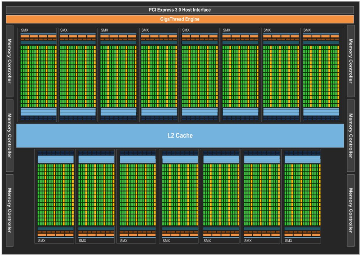
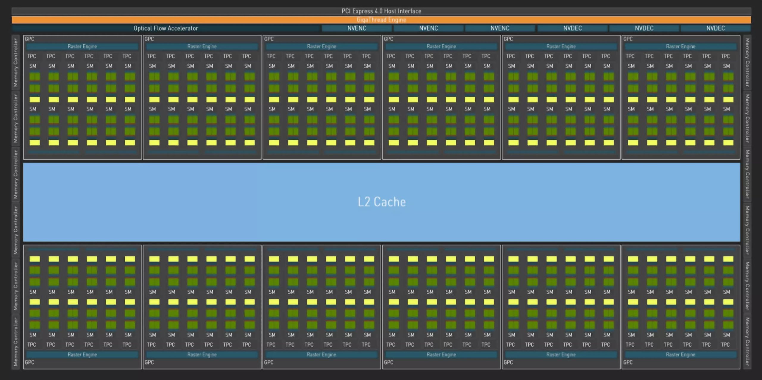
Turing architecture brought many changes to GPUs. For example, the block diagram of the TU102 GPU used in high-end graphics cards looked like below.
Number of CUDA Cores per SM reduced to 64 (from 128). Added Tensor Kernels and Ray Tracing Kernels. The company switched to TSMC’s 12nm production technology. Also, starting from the Turing architecture, integer and floating point units were separated.
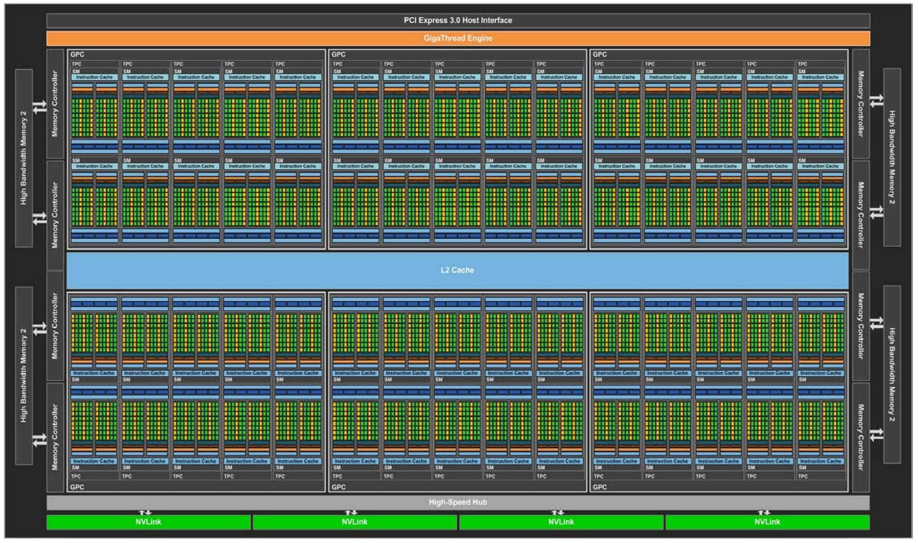
Ampere architecture introduced 2nd Generation Ray Tracing Cores. The GA100 GPU had 128 SM. Ampere GA102 has 10,752 CUDA cores. This time, each core consisted of two FP32 processing units (units that perform 32-bit floating point operations).
The interesting thing about Ampere CUDA cores is that it can perform operations on both integers and floating points. This means that each CUDA core in the Ampere architecture can handle two FP32 or one FP32 and one INT operations per clock cycle.
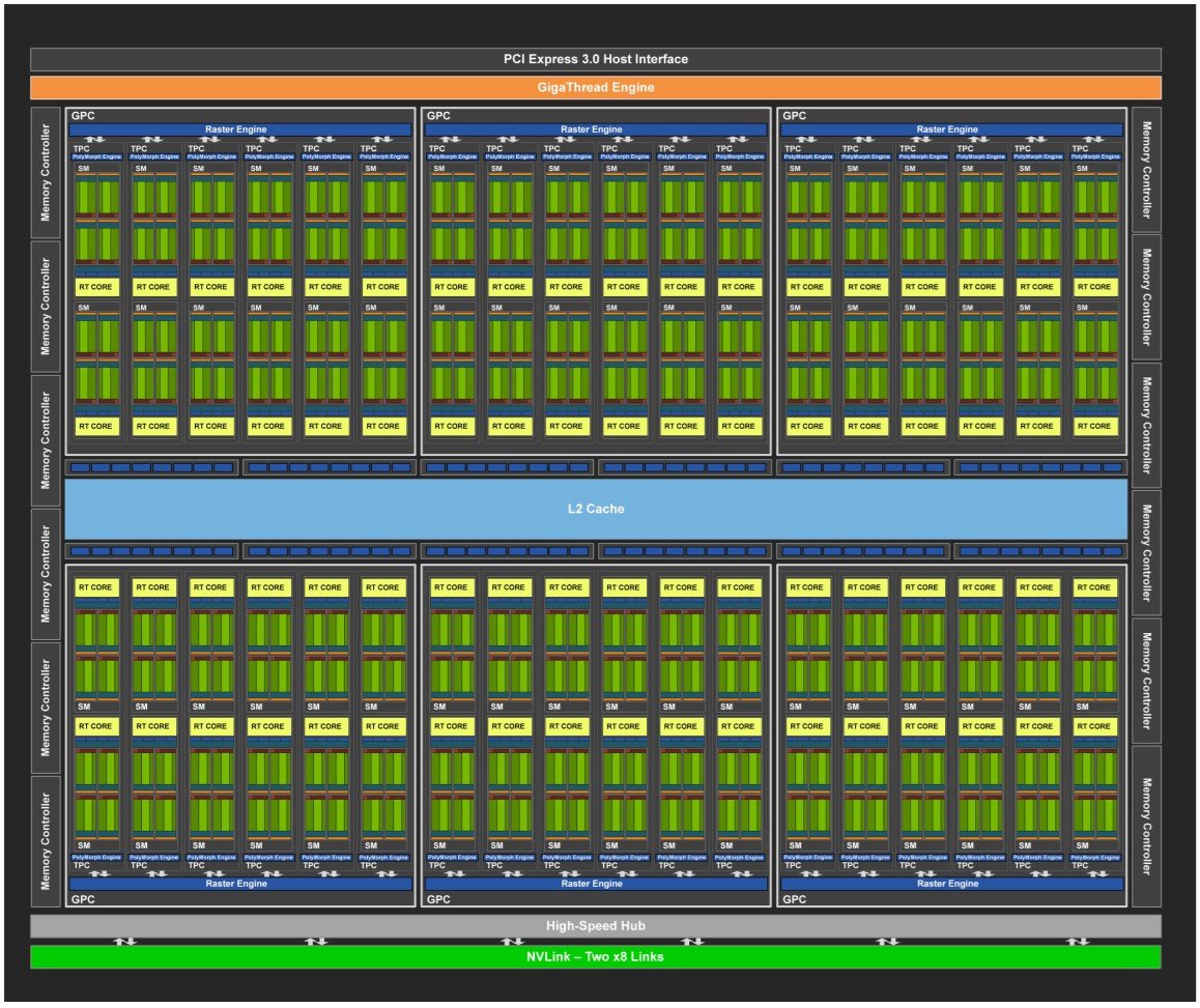
While writing these words, Ada Lovelace’s architecture was the green team’s strongest trump card. NVIDIA continues the design process with Graphics Processing Clusters (GPC), which includes 6 Texture Processing Clusters (TPC). Each of these contains a Streaming Multiprocessor (SM). Although the configuration did not change with Ada Lovelace, there was a change in the total figures.
The number of GPCs increased from 7 to 12 on the untrimmed AD102 graphics die. Thus, it became possible to build a GPU with a total of 144 SM and 18,432 CUDA cores. Compared to Navi 31’s 6144 SP, 18,432 may seem like a huge number, but as we said, the design is very different.
On the other hand, we also saw different changes in architecture. 4th generation Tensor Cores started to be used along with 3rd generation Ray Tracing Cores.
Although previous generation Ampere graphics cards offered AV1 decoding support, AV1 encoding support was not offered. Graphics cards built on Ada architecture have the eighth generation NVIDIA Encoder (NVENC) that offers AV1 coding support.
Why are CUDA Kernels Important?
CUDA Cores are the heart of NVIDIA GPUs. These cores are used to process and render images, videos, and other visual information for both display devices such as monitors and TVs, and computer vision applications. It’s happening.
Each new generation of NVIDIA GPUs comes with more powerful cores. The company’s newest flagship GPU, GeForce RTX 4090, has 16,384 CUDA cores. In other words, an increase of approximately 40% compared to the previous generation, and that’s a lot of power!
GPUs with large numbers of CUDA cores can perform certain types of complex calculations much faster than GPUs with fewer cores. Of course, the number of cores is not the only factor, but we wouldn’t be wrong if we said it is the most important factor. As a matter of fact, CUDA cores are an important criterion to comment on the performance of an NVIDIA GPU.
Let’s give a summary. CUDA cores are the parallel computing workhorse of modern NVIDIA GPUs. Therefore, they have a significant impact on the performance of a GPU. These cores enable the GPU to take computation-intensive tasks from the CPU and process them on CUDA cores.
CUDA cores also contribute to general-purpose GPU computing (GPGPU) and graphics rendering. Therefore, CUDA Cores are a very important performance criterion that greatly affects the performance of a graphics card.
In Which Tasks Is It Used?
CUDA Cores play a huge role in modern NVIDIA GPUs. It is active in executing parallel computation as well as facilitating various other tasks. Some of the important roles of these nuclei are as follows:
- Parallel Processing: CUDA Cores are designed to perform parallel processing tasks efficiently. While the CPU workload is lightened, the GPU is enabled to perform multiple calculations at the same time. Moreover, it has become possible to execute complex calculations in a fraction of the time it would take to be performed by the CPU alone.
- Graphics Processing: CUDA Kernels were initially developed for graphics processing. Apart from parallel computing, we can show these cores as the backbone of GPU-based rendering. Various graphics-related tasks such as vertex rendering, pixel shading, geometry rendering, and texture mapping take place here. On the other hand, CUDA cores are excellent at rendering realistic 3D graphics, enabling fluid and immersive visual experiences in gaming, virtual reality and computer-aided design (CAD).
- General Purpose GPU Computing (GPGPU): CUDA cores to accelerate a wide variety of computing tasks beyond graphics including scientific simulations, machine learning, data analytics and much more get in available. By leveraging the parallel processing power of CUDA cores, complex calculations can be broken down into smaller, parallel tasks that execute simultaneously, which is incredible. ¼ provides performance gains.
- CUDA Toolset and Programming: If you are a developer, you can use CUDA Toolkit, which contains programming models and libraries for GPU programming. With the help of this toolset, you can write codes that run only on CUDA-enabled GPUs. You can harness the power of CUDA cores and unlock the parallel processing capabilities of GPUs.
How Do CUDA Cores Affect Performance?
We said that every NVIDIA GPU contains hundreds or thousands of CUDA cores. When it comes to processing power, there are many things to consider when evaluating the performance of a GPU. GPU clock speeds, GPU architecture, Memory bandwidth, Memory speed, TMUs, VRAM and ROPs are some of the other factors that affect GPU performance.
VRAM holds objects, textures, shadow maps, and any other data processed through the GPU. The reason why graphics cards store this data in VRAM is that it is much faster to access it from VRAM compared to DRAM, SSD or HDD.
When it comes to clock speeds, there are two things we need to discuss: the core clock and the memory clock. Core clock is the speed at which the GPU operates. On the other hand, memory clock is the operating speed of the GPU VRAM. The core clock is similar to the clock speed of the processor, and the memory clock is similar to the speed of the system RAM.
Most CPUs in the mainstream market come with two to sixteen cores. The increase in the number of cores allows them to perform operations in parallel, albeit partially. When it comes to graphical calculations there are a lot of things that need to be calculated in parallel. When you look at GPUs, what you call a core is actually just a Floating Point Unit for CPUs.
A GPU core cannot fetch or decode instructions, it only performs calculations. The number of cores we mentioned is now expressed in thousands in modern GPUs.
It is not possible to evaluate the performance of any graphics card only by the number of CUDA cores. You need to take into account the architecture of the graphics cards, their clock speeds, the number of CUDA cores and much more that we mentioned above.
If you are comparing GPUs within the same generation, the CUDA count can be a good indicator of performance. For example, GTX 960 has 1024 CUDA, while GTX 970 has 1664 CUDA cores. GTX 970 carries more CUDA cores and is much more performant compared to its little brother GTX 960.
More number of CUDAs means better performance unless there are other factors that reduce performance. When you compare graphics cards of different generations and architectures, things get a little confusing. For example, GTX 1070 has almost the same number of CUDA cores as GTX 780. On the other hand, RTX 2060 has fewer CUDA cores compared to GTX 780. As you know, these figures do not show that the GTX 780 is superior to the GTX 1070 or RTX 2060.
The difference in performance arises due to different architecture, efficiency improvements, performance improvement, instruction sets, transistor size and manufacturing process between different generations of GPUs. The performance of the CUDA kernel greatly depends on the fabrication size and GPU architecture. In summary, we can say that a single CUDA core of the new generation can be much more powerful compared to the previous one.
Let’s consider two GPUs from different generations, the GTX 980 Ti based on Maxwell architecture and the GTX 1080 based on Pascal architecture:
| GeForce GTX 980 Ti | GeForce GTX 1080 | |
| Number of Transistors | 8,100,000,000 | 7,200,000,000 |
| Number of CUDA | 2816 | 2560 |
| Number of Transistors/Core | 2,876,420 | 2,812,500 |
| Clock Speed | 1500MHz | 2000MHz |
When you look at the table above, you can see that there is a slight difference in terms of transistor/CUDA core between the two graphics cards. If you look at the numbers you might think that performance would be similar, but that’s a false conclusion.
The small size of the transistors in the Maxwell architecture is what makes the difference here. Smaller transistors reduce overall power consumption and allow manufacturers to pack more transistors into a small die. All of this leads to an increase in the maximum clock frequencies that Pascal GPUs can reach, which increases overall performance.
To find out how good your GPU is, we recommend looking at real-world gaming or computing benchmarks rather than getting caught up in the intricate details. You can find reviews of graphics cards from every segment on Technopat.Net. Here are the CUDA values of the last generation NVIDIA graphics cards:
| Graphics Card | Number of CUDA Cores |
|---|---|
| RTX 4090 | 16384 |
| RTX 4080 | 9728 |
| RTX 4070 Ti | 7680 |
| RTX 4070 | 5888 |
| RTX 4060 Ti | 4352 |
| RTX 4060 | 3072 |
| RTX 3090 Ti | 10752 |
| RTX 3090 | 10496 |
| RTX 3080 Ti | 10240 |
| RTX 3080 | 8960 |
| RTX 3070 Ti | 6144 |
| RTX 3070 | 5888 |
| RTX 3060Ti | 4864 |
| RTX 3060 | 3584 |