
NVIDIA officially announces next-generation Blackwell GPU architecture that delivers up to 5x AI performance boost over Hopper H100 GPUs introduced. The new architecture stands out with 208 billion transistors, 192 GB HBM3e memory and 8 TB/s bandwidth. Blackwell is 7 to 30 times faster than the H100 and uses 25 times less power.
NVIDIA Blackwell Features
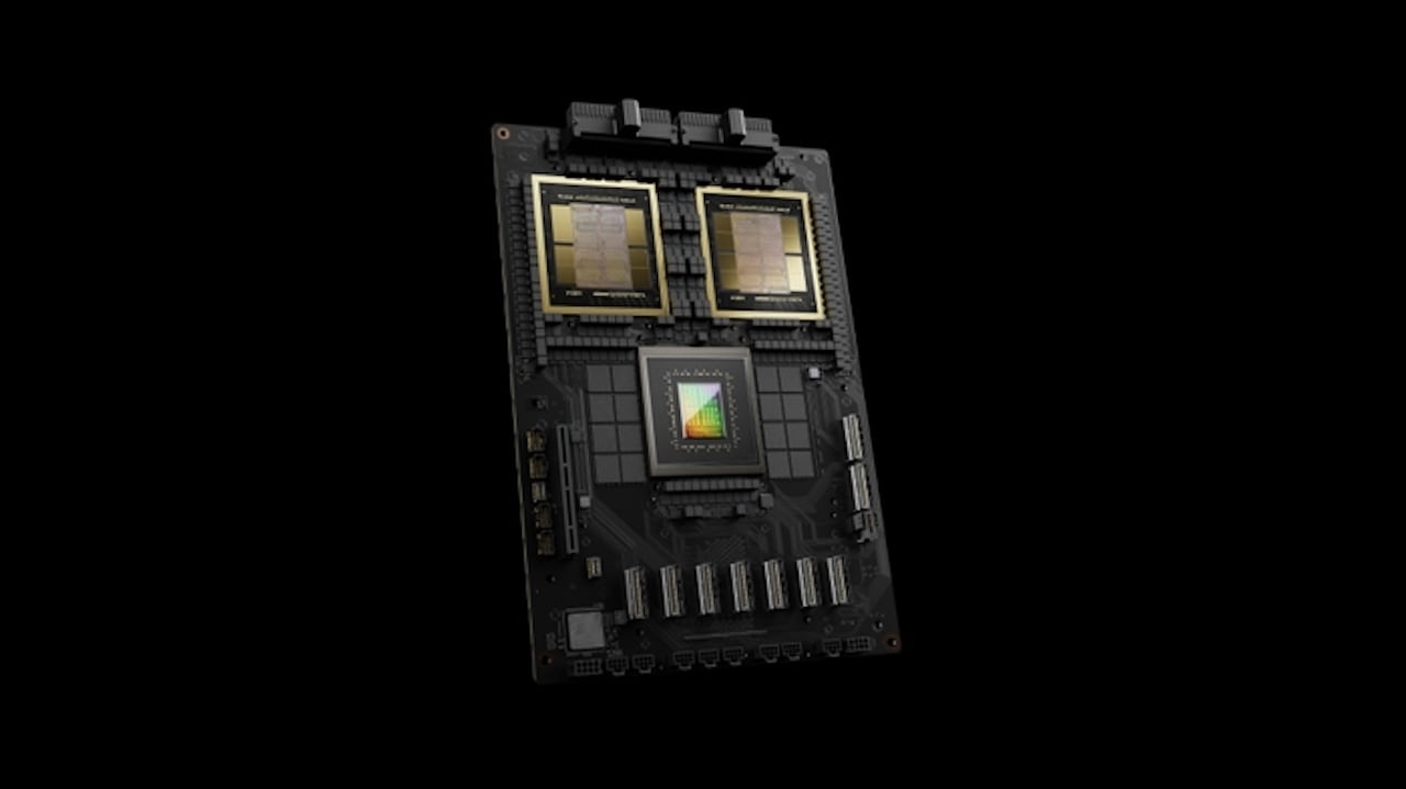
NVIDIA has formalized its next-generation artificial intelligence and Tensor Core GPU architecture, codenamed Blackwell, in full detail. As expected, the Blackwell GPUs are the first GPUs to feature NVIDIA’s MCM design, which includes two GPUs on the same die.
Blackwell’s features are listed as follows:
- TMSC 4NP Processing Node
- Multi-Chip Package GPU
- 1-GPU 104 Billion Transistors
- 2-GPU 208 Billion Transistors
- 160 SM (20,480 Cores)
- 8 HBM Packages
- 192GB HBM3e Memory
- 8 TB/s Memory Bandwidth
- 8192-bit Memory Bus Interface
- 8-Hi Stack HBM3e
- PCIe 6.0 Support
- 700W TDP (High Point)
- The World’s Most Powerful Chip – Packed with 208 billion transistors, the Blackwell architecture GPUs are manufactured using a custom-built 4NP TSMC process with two reticle-limit GPU dies connected to a single, unified GPU via a 10TB/second chip-to-chip connection.
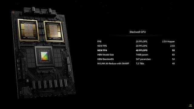
- Second Generation Transformer Engine – Powered by new micro-tensor scaling support and advanced dynamic range management algorithms integrated into NVIDIA’s NVIDIA TensorRT-LLM and NeMo Megatron frameworks, Blackwell will support twice the compute and model sizes with new 4-bit floating point AI inference capabilities.
- Fifth Generation NVLink – To accelerate the performance of multitrillion-parameter and expert-mix AI models, the latest iteration of NVIDIA NVLink delivers a breakthrough 1.8 TB/s bidirectional throughput per GPU, enabling seamless high-speed communication between up to 576 GPUs for the most complex LLMs.
- RAS Engine – Blackwell-powered GPUs include a proprietary engine for reliability, availability and serviceability. Additionally, the Blackwell architecture adds chip-level capabilities to run diagnostics and use AI-based preventive maintenance to predict reliability issues. This maximizes system uptime and increases flexibility for large-scale AI deployments to run uninterrupted for weeks or even months at a time, reducing operating costs.
- Safe Artificial Intelligence – Advanced confidential computing features protect AI models and customer data without compromising performance by supporting new native interface encryption protocols that are critical for privacy-sensitive industries such as healthcare and financial services.
- Decompression Engine – Special A decompression engine supports the latest formats, accelerating database queries to deliver the highest performance in data analytics and data science. In the coming years, data processing on which companies spend tens of billions of dollars each year will increasingly be accelerated by GPUs.
NVIDIA hasn’t announced how much the Blackwell chips will cost. H100 chips, on the other hand, currently cost between $25,000 and $40,000 per chip, and entire systems powered by these chips can cost up to $200,000. Let us remind you that NVIDIA chips are in high demand despite their high costs.