
We examine transistors, which can be called the smallest component of the technological devices we use today, and which are considered one of the best inventions in the history of science and engineering. Although we sometimes talk about it, we do not know in detail what these tiny electronic parts do, how they work, and how they are used in chips. We haven’t covered it yet.
Transistors are considered the “key” component that enables the electronic devices we use today to operate. It is one of the types of semiconductor devices used to transmit/insulate electric current or voltages. In other words, we can say that it is the most basic electronic part that can amplify and change electronic signals and electrical power. We are talking about semiconductors that control the flow of current between their terminals depending on the voltage applied to them. In simple terms, it acts as a small electronic switch or an amplifier.
If there were no transistors, the chips you see in all kinds of technological devices would not exist. Let’s take a closer look at the “most basic component” that comes to mind when we say electronics and technology.
What is Transistor?
Transistors, the basic building blocks of electronic devices, are semiconductors that amplify or change electronic signals and electrical power. The most important basic component in almost all electronic devices, including computers, smartphones and digital watches.
The importance of conductors, which we call transistors, in modern electronics is so great that let us remind these words again: It is accepted as one of the best inventions in the history of science and engineering. While technology was being revolutionized, miniaturization of electronic devices was achieved, so producing smaller, faster and more energy efficient products is no longer a dream. It was gone.
Countless devices have been developed thanks to transistors that provide the functionality of integrated circuits, which are the heart of all digital devices. From radios and televisions to computers and mobile phones, these small parts are integral to daily life. on our lines It made a significant impact. In addition, microprocessors play a very important role in the advancement of technology by enabling the development of digital signal processing and data storage.
![]()
It is safe to say that transistors have made the digital age possible. Without them, the technological advances we enjoy today would not be possible. Maybe you wouldn’t even be reading these words on your palm-sized smartphone or powerful computer. Therefore, in order to master modern technology, it is necessary to understand how transistors work and their role in electronics.
A transistor has only one circuit element by itself. Small amounts of transistors are used to create simple electronic switches. They are the basic elements of integrated circuits (IC), which consist of many transistors connected to each other by circuits and placed inside a single silicon microchip.
It is possible to place millions, and today even billions, of transistors into a single integrated circuit. These types of chips produced with high technology are much more performant and more efficient. Conductors are used not only in processors, but also in storage units in countless products, including MP3 players, smartphones and cameras. RAM technologies that offer temporary storage also include chips, that is, the transistors required to form chips.
Brief History
The history of transistors dates back to the early 20th century. The first transistor was invented in 1947 at Bell Laboratories in the United States by a scientific team consisting of William Shockley, John Bardeen and Walter Brattain. This invention was a tremendous breakthrough in electronics that ignited the semiconductor era.
The transistor was a revolutionary invention because it offered a more reliable and compact alternative to the vacuum tubes used in electronic devices at that time. Vacuum tubes were bulky, consumed a lot of power, and had a limited lifespan. However, transistors were much smaller, required less power, and had a much longer lifespan. In short, it was ideal for use in electronic devices in different fields.
The first transistors were made of germanium, which was readily available at the time. However, the cost of germanium was high and it performed poorly at high temperatures. Afterwards, in the 1950s, researchers began to investigate the use of silicon as an alternative to germanium. Silicon had several advantages over germanium, such as a higher melting point and better electrical properties. By the late 1950s, silicon became the material of choice for transistor manufacturing.
![]()
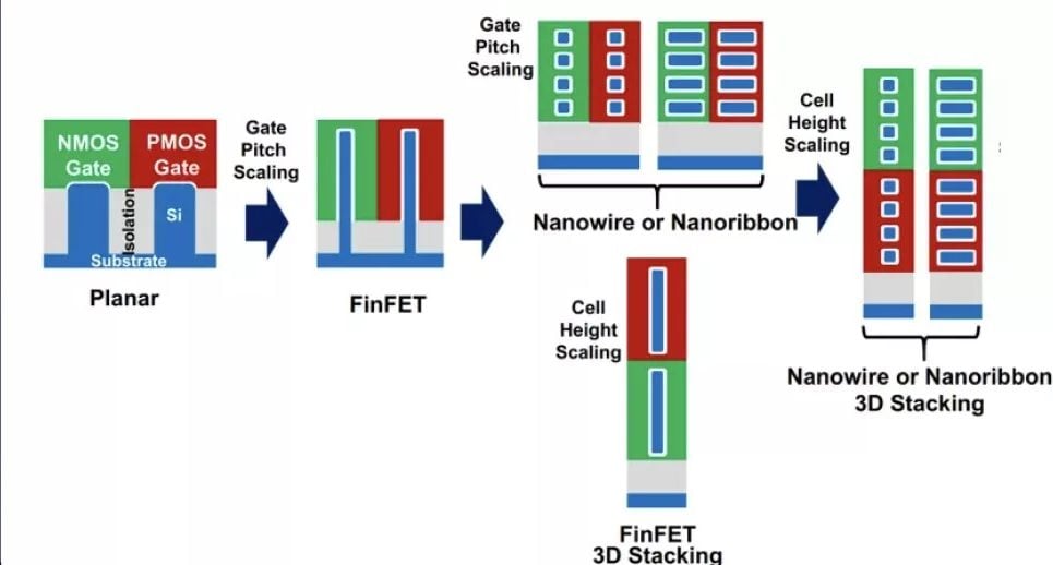
As the size of transistors has decreased exponentially, their cost has also decreased, creating more opportunities to use them. Integrating transistors with resistors, other diodes or electronic components has made integrated circuits smaller. While talking about miniaturization and semiconductors, we can’t not mention Moore’s Law. We’ll talk about it in a moment.
The invention and subsequent development of the transistor had a profound impact on the evolution of modern electronics. We can say that these conductors are the primary factor that enables the development of integrated circuits and microprocessors by enabling the miniaturization of electronic devices. When we look at it in general, as a result of all the developments, the digital age has opened up and the world has undergone a great change. From computers and smartphones to medical devices and space exploration, transistors have played a key role in shaping the world we know today.
Transistor Materials and Manufacturing Process
The materials and manufacturing processes used to produce transistors are of critical importance in terms of their performance and functionality. Silicon, a semiconductor, is the most widely used material in transistor production due to its excellent semiconductor properties, abundance in nature, and relatively low cost. It has a crystalline structure that allows the controlled entry of foreign substances, a process known as doping, which is crucial for the operation of transistors.
Doping involves “processes of introducing impurities” into silicon to change its conductivity. There are two types of doping: n-type, in which dopant atoms have more valence electrons than silicon, and p-type, in which dopant atoms have fewer valence electrons. The interaction between n-type and p-type materials in a transistor allows electrical signals to be controlled and amplified.
The manufacturing process of transistors is quite complex and has multiple stages. The process begins by creating a wafer (silicon disk sheet), which is a thin slice of silicon crystal. The wafer is then subjected to various processes such as oxidation, photolithography, etching (or etching) and diffusion or ion implantation to create the structure of the transistor. Through oxidation, a silicon dioxide layer, which acts as an insulator, grows on the wafer. Photolithography is used to transfer the transistor’s pattern onto the wafer. During the etching process, unwanted materials are eliminated to reveal the structure of the transistor, while additives are incorporated into the silicon by diffusion or ion implantation.
As for the final steps, metal contacts are placed to connect the transistor to the rest of the circuit, and the completed transistors are packaged for use in electronic devices. The entire process negatively affects the performance of the transistor. contamination that may affect It is carried out in a clean room environment to prevent
![]()
Over the years, the manufacturing process of transistors has improved significantly thanks to technological advances, enabling the production of increasingly smaller, more powerful transistors. outside. Nowadays, transistors are developed using technology such as FinFET (Fin Field Effect Transistor) and GAAFET (Gate-All-Around Field Effect Transistor) that allow the production of transistors with features as small as a few nanometers. sophisticated techniques It is produced using .
These advances in materials and manufacturing processes have played a key role in the ongoing evolution of transistor technology, enabling the development of increasingly powerful and energy-efficient electronic devices.
Working Principle of Transistors
Transistors work according to the principles of semiconductor physics. At the core of these principles is the concept of “charge carrier”, which can be an electron or a hole (absence of electrons). The behavior of charge carriers in the semiconductor material of a transistor allows them to control and amplify electrical signals.
Typically, a transistor consists of three semiconductor material layers: emitter, base and collector. The emitter and collector are generally heavily doped, meaning they have a high concentration of charge carriers, while the base is lightly doped. The emitter and collector belong to one dopant type (n-type or p-type), while the base belongs to the other type.
The operation of a transistor occurs through a base-emitter combination that acts as a gate. By applying a small current to the base, it allows a much larger current to flow from the emitter to the collector. This is the amplification effect of a transistor.
The base-emitter junction can also act as a switch. When no current is applied to the base, the junction prevents current from flowing from the emitter to the collector, and when a current is applied to the base, it prevents current from flowing. It allows ±. This switching property is what makes transistors so valuable for digital electronics.
![]()
The operating principles of the transistor are the same for all transistor types, but the characteristics may vary depending on the transistor type and intended application. Regardless of the type, charge carrier behavior and basic principles of doping and coupling make transistors a powerful tool in electronics.
How does it work?
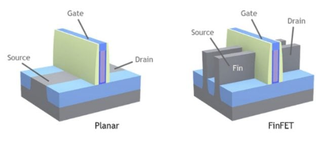
A transistor is essentially a switch that can control the flow of electrical current. There are three terminals:
- Bipolar Junction Transistor (BJT) type emitter, base and collector.
- In Field Effect Transistor (FET) type transistors, source, gate and drain.
The behavior of the transistor depends on the voltages applied to these terminals. In a BJT, a small current applied to the base-emitter junction allows a much larger current to flow from the emitter to the collector. This current amplification is an important feature of BJTs. The ratio of the output current (collector current) to the input current (base current) is called current gain and is symbolized by the symbol β. ¶required.
- Base: To enable the transistor
- Collector: Positive end of the transistor
- Emitter: Negative end of the transistor
The flow of charge carriers between the source and drain terminals of a FET type transistor is controlled by an electric field created by applying a voltage to the gate terminal. Unlike BJTs, FETs do not require a base current to operate, making them more energy efficient.
![]()
Thanks to the ability of transistors to control the flow of electric current, it is possible to use them in a wide variety of areas. We can use it to amplify signals, as in audio amplifiers and radio transmitters, or to switch signals on and off, as in digital circuits. By combining millions or even billions of transistors on a single chip, complex electronic devices such as microprocessors and memory chips can be designed.
![]()
What is the Function of the Emitter?
The emitter, known as the emitter or emitter, is responsible for emitting or injecting the majority charge carriers (electrons or holes) into the base region of the transistor.
What is the Function of Some?
Base is another terminal of a transistor. Its main function is to control the current flow between the emitter and collector. By applying a small current or voltage to the base, you can control a much larger current flowing through the transistor.
What is the Function of the Collector?
The collector collects the majority charge carriers emitted by the emitter and controls the current flow through the transistor. The collector is generally designed to handle larger currents compared to the emitter and base.
Development Process and Modern Transistors
Following the invention of the point-contact transistor in 1947, the electronics field entered a period of rapid change and innovation. However, although the point-contact transistor was revolutionary, it was difficult to produce reliably and was not suitable for mass production. As a result of these disadvantages, junction transistors, which are a more reliable and easier to manufacture design, were developed in the early 1950s.
Junction transistor, a three-layer device in which a thin layer of one type of semiconductor material is sandwiched between two thicker layers of another type, point contact li It was more robust and reliable than the transistor. As a result, it quickly became the standard for transistor design.
Significant breakthroughs were made in the 1950s and 1960s with the development of the bipolar junction transistor (BJT) and the field effect transistor (FET)4. It works with a different principle. While the BJT is a three-layer device, the FET is a four-layer device that controls the width of a ‘channel’ through which current flows.
![]()
The development of these new types of transistors opened up new possibilities for electronic design. Small semiconductors could now be used not only to amplify signals but also to switch them on and off, making digital electronics possible. This progress enabled transistors and other components to be assembled on a single chip in 1958 and opened the door to the development of integrated circuits. By the 1960s, integrated circuits were developed. very diverse It was used in electronic devices.
The evolution of the transistor continued, with the metal-oxide-semiconductor field effect transistor (MOSFET) being developed in the 1970s. It has become the most common type of transistor used today because it has several advantages over previous options. For example, it is easier to produce, can be made very small and consumes very little power.
While transistors are now present in every aspect of modern electronics, their evolution is not over yet. Semiconductor companies that shape the future of the technology world are starting to make future plans long in advance. Here are some of these examples:
First GAA Transistors: Samsung Begins 3nm Production
Samsung announced that it started chip production using 3nm production technology with Gate-All-Around (GAA) process technique in late 2022. The 3nm process will deliver 45% reduced power usage, 23% improved performance and 16% smaller surface area compared to the 5nm process. In the second generation 3nm process, these values will be increased to 50%, 30% and 35% respectively.
![]()
The Korean semiconductor manufacturer, which has reached the end of the limits for FinFET, aims to exceed the performance limits with Multi-Bridge-Channel FET (MBCFET), the GAA technology applied for the first time. With the new technique, while the supply voltage level is reduced, power efficiency increases to a higher level. At the same time, performance increases with the drive current capacity.
Samsung brands its 3GAE omnidirectional field-effect transistors (GAAFETs) as multi-bridged channel field-effect transistors (MBCFETs). The low leakage current of the transistors stands out as one of the key features as the gate is now surrounded by the channel on all four sides. Another advantage is that the thickness of the channels can be adjusted to increase performance and reduce power consumption.
![]()
The term “primary production” can be interpreted differently. The semiconductor giant was in the early start-up phase of mass production in late 2022. But Samsung Foundry can be officially branded as the world’s first chipmaker with gate-all-around (GAA) transistors.
2nm Chip Production May Start in 2024: MBCFET Transistors
TSMC has started to build a production facility for 2nm technology and it is planned to use the MBCFET transistor structure. Taiwan Semiconductor Manufacturing Company made a significant breakthrough in research and development for 2nm semiconductor manufacturing technologies in 2020. Reports of this breakthrough surfaced in the Taiwanese media. TSMC, which supplies chips to various large and small companies around the world, expects this process to enter trial production in 2023 and serial production a year later. waiting for production to start.
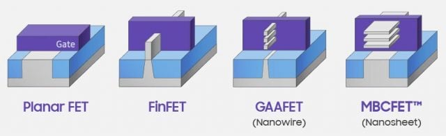 FinFET (Fin-Field Effect Transistor) technique, a term used to describe the design of a transistor, is used in products manufactured by TSMC and Samsung. TSMC, on the other hand, aims to switch to a model called Multi-Bridge Channel Field Effect (MBCFET) transistor.
Transistors – FinFET, GAAFET, MBCFET
A FinFET design depends on three basic elements. These are called source, gate and drain. After the electrons leave the source, their flow is regulated by the gate. In designs before FinFET, sources and channels were produced only in the horizontal axis. MBCFET is a kind of continuation of FinFET.
FinFET’s innovative approach enabled vertical positioning of both sources and channels in the third dimension. As a result, more electrons were able to pass through the gate, leakage was reduced and the operating voltage was reduced.
 TSMC’s decision to use an MBCFET for its transistors is not actually a first. As we mentioned, Samsung announced the 3nm manufacturing process and the MBCFET design was mentioned. Unlike GAAFET, Samsung’s MBCFET uses nanowire instead of “nanosheet” sources and channels. This innovation increases the surface area available for conduction and, more importantly, allows the designer to add more gates to the transistor.
Intel is working on Sub-2nm Transistor Technology
Intel is focusing on a new transistor design aimed at sub-2nm production targets for use in future products. An online patent published in 2022 had emerged. Given this, the company wants to keep Moore’s Law alive through an approach it calls “stacked forksheet transistors.” As is usually the case, the patent is vague and makes no claims about Intel PPA (Power-Performance-Area) improvements.
According to the blue giant, the new transistor design is 3D, which allows for a greater number of transistors than today’s most advanced three-gate designs. a stacked CMOS architecture It endures. On the other hand, miniaturizing transistors is becoming very difficult, and even Intel’s patent describes the difficulties encountered as “overwhelming.” It looks like the cost, risk and complexity now seem to outweigh the potential benefits.
Intel’s patent reveals the use of nanostrip transistors paired with a new, atom-thin germanium film that acts as an insulating wall. This wall acts as a physical separator between the layers and also as an insulator between the p-gate channel and the n-gate channel. It is also repeated across each of the vertically stacked transistor layers depending on how many transistors are stacked on top of each other.
As a result, the technology giant will be able to fit many more transistors into a narrower space. The company started exploring the technology in 2019 and first announced this development at the Electronic Devices Meeting (IEDM) event. Unfortunately, there is no concrete data on any patent and technology-related issues such as transistor density, performance and power efficiency.
It is worth remembering that not all patents always turn into real products or production technologies over time. However, the technology world will need 2nm and below technologies sooner or later. In addition to Intel, foundries such as TSMC and Samsung are also working hard to develop their own technologies.
Intel may also use other techniques instead of this “stacked forksheet” architecture in the 2nm process. However, the company has applied for a patent, which ultimately means the design has validity.
Processors with 300 Billion Transistors Could Be Produced by 2030
The company, one of the important names behind semiconductor production, will ensure that Moore’s Law lives a little longer. ASML Holding is an important company responsible for the design and installation of machines used in the production of silicon chips. The Dutch tech firm has laid out plans to create processors that will have more than 300 billion transistors by 2030 in a document for investors.
![]()
Of course, obtaining the mentioned 300 billion transistor value is not an easy task. However, there is a solid basis for the 300 billion target. The company plans to achieve this development process by dividing it into two stages; The first is increased transistor density, and the second is an improved packaging process.
![]()
First of all, transistor density is very important. They plan to use nanosheet-FETs with a combination of extreme ultraviolet (EUV) lithography for production technologies below the current 5nm technology, such as 3nm and 2nm. What comes next is a difficult road to the 1.5nm node and requires bifurcated nanolayers. Additionally, CFET technology is expected to be preferred to achieve 1nm production. ASML will use 2D atomic channels for sizes below 1nm.
![]()
ASML wants to apply advanced packaging techniques to combine chips and build multi-chip modules (MCM) as high-transistor chips become the standard. Ultimately, processors with more than 300 billion transistors will emerge. As a result, 3D and logical stacking will play an important role in heterogeneous processor design and the production of layered I/O systems.
![]()
The Future of NAND Chips
When it comes to memories, future techniques will enable memory manufacturers to produce NAND flash modules with more than 500 layers by 2030. Today’s advanced NAND modules are shipped with around 200 layers.
Semiconductors
Semiconductors form the basis of modern electronics due to their electrical conductivity intermediate between conductors and insulators. We said that the most commonly used semiconductor material in transistors is silicon, but other materials such as germanium and gallium arsenide are also used in some applications.
The electrical properties of semiconductors are regulated by a process known as doping. We have just mentioned the doping process. With this process, the entry of foreign substances is allowed in a controlled manner, and the purity of the substance is changed. Small amounts of other elements can be added to the semiconductor material and an excess or deficiency of electrons is created.
Transistors take advantage of the properties of semiconductors to control and amplify electrical signals by alternating n-type and p-type layers in a three-layer configuration. The interaction between the layers and the flow of electrons and holes (holes) within them enable transistors to function as amplifiers or switches.
In a transistor, the flow of charge carriers (electrons or holes) between layers is controlled by a voltage applied to one of the layers, called the base. By varying the voltage at the base, the current flowing between the other two layers, the emitter and collector, can be controlled. This allows the transistor to amplify or switch electrical signals, making it a fundamental building block of modern electronic devices.
What is Semiconductor Manufacturing Technology?
In English sources, you can see terms such as “process node”, “process technology”, “technology node” and just “node”. They all lead to the same door. The word “node” means “node”. We can use this as a “circuit node”. As you know, the transistors on the chips are extremely close to each other, on the scale of nanometers. We can define this structure as a “node” because they come one after the other. However, we generally prefer to use clearer terms such as process technology, production technology and fabrication technology.
Process node refers to a specific semiconductor manufacturing process and the design rules of this process. Nodes in ip production include interconnection range, transistor density, Type and other It shows the features that the production line can create on an integrated circuit, such as new technologies.

The production techniques called 5nm and 7nm are related to the “chip production” processes that take place in production facilities, which we also call foundries. Although almost all chips are produced using silicon, there are different manufacturing processes that foundries can use. That’s why we use the word “process”. In summary, when silicon chips are produced, the size of the transistor components is measured, and with these dimensions, “special” production methods emerge.
Processors consist of many transistors, expressed in billions, and the more transistors inside a processor, the better. So how can we get so much performance by placing unlimited transistors? Unfortunately, goals in the world of technology do not progress in this direction. We can call the concept of “miniaturization” in the design and advancement of integrated circuits. Giants, which have been in the foundry business for years, continue to reduce the transistor range relentlessly. Process technologies are being developed with the aim of endlessly “making smaller”.
If a large number of transistors were placed without miniaturizing the process technologies, we would be using huge processors reaching gigantic sizes. Thus, heat production would increase greatly and we could not use small technological devices. Technology Companies strive to pack more transistors on a chip by reducing the gap between transistors to increase density. As newer and better processes are invented, transistor density increases, efficiency increases, space becomes smaller, and we can achieve performance without the need for large chips.
The World’s First Wooden Transistor Developed: 1 Hz Speed
Researchers continue their work to make new discoveries. Researchers in Sweden designed and tested the world’s first wooden transistor. Linköping UniversityTeams from  and the Royal Institute of Technology in Stockholm have recently created a paper showing the development process, capabilities and potential of their wooden electrochemical transistor (WECT). article published.
![]()
Wood electrochemical transistors could pave the way for more sustainable and biodegradable wood-based electronics. Moreover, wood electronics can provide electronic control of living plants.