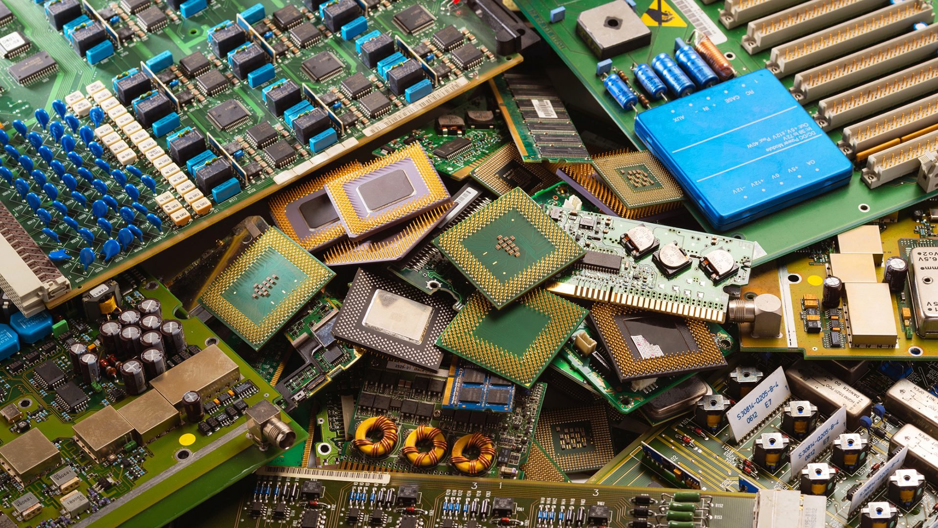

There are many chips, large and small, in countless products that we use in our daily lives, including computers, phones, watches, small household appliances and automobiles. In addition, it plays a critical role in many fields, including aircraft, defense industry and medical devices. The production of chips, which find a place in every aspect of life and whose importance increases day by day, is a very arduous task. You may be familiar with the constantly evolving semiconductor production technologies. At least when buying a product, you will see terms such as 10nm, 7nm and 3nm. What are these?
We encounter the names of semiconductor technologies more often, especially when purchasing products such as processors, graphics cards, laptops, tablets and smartphones. Like many technical features, the processing technologies known as “process nodes” are a term that most people do not understand. Actually, it is not something that you should care too much about as an end consumer, but it is a term that many people do not understand. It is an important factor when it comes to technology and chips. It’s even directly related to the chip production itself.
We often talk about production technologies in our articles and videos. Although things like 7nm and 5nm are mentioned frequently, we miss what they technically mean. Now, as we speak, we will try to shed light on the details about process technologies and chips.
What Does “Nm” Mean?
65nm, 32nm, 10nm, 5nm… As the years change, foundry technologies also change. All chips, including processors produced by Intel and AMD, SoCs and NVIDIA GPUs in Apple and Samsung smartphones, are produced with these processes. TSMC, Intel and Samsung are the largest foundries producing chips. Companies such as AMD and NVIDIA are actually called “chip manufacturers”, but they do not have their own foundries or production facilities. They design the chips and outsource their production to giants like TSMC.
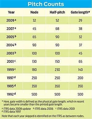
Process technologies are often named with a number followed by the nanometer abbreviation: 22nm, 14nm, and 7nm. In recent years, this tradition has begun to change. There is no fixed, objective relationship between any feature of the CPU and the name of the technology. This wasn’t always the case. From approximately the 1960s until the late 1990s, technologies were named according to their gate lengths. This table from IEEE shows the relationship:
 Since 2017, the way semiconductor production technologies are named has also begun to change. So what’s the reason for this? The size, density and performance of transistors are no longer matched between foundries. For example, Intel’s 10nm is comparable to other foundries’ 7nm, while 7nm processes are comparable to other companies’ 5nm technologies At a breakable level.
Nomenclatures Are Changing
Intel ended the nanometer naming in 2021. While AMD switched to 7nm TSMC production, Intel continued with 14 nm+++. For this reason, the following perception began to emerge among the buyer audience in the processor market: “While AMD was 7nm, Intel still had 14 nm left, and even could only produce a 10 nm processor in such a long time.”
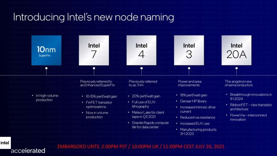
However, this did not have any truth, the 10 nm production technology that Intel planned to switch to in the next generation was already close to TSMC’s 7nm technology. For this reason, Intel continued to lose market share, and long discussions about nanometers arose in forum rumors. That’s why Intel is updating the manufacturing terminology it uses for its semiconductor processes to match TSMC manufacturing.
Are Intel 10nm and TSMC/Samsung 7nm Technologies Equivalent?
There is such a debate on the internet and there is a reason for this. The manufacturing parameters for Intel’s 10nm process are very close to the values used by TSMC and Samsung for what they call the 7nm process. The table below, taken from WikiChip, compares known feature sizes for Intel 10nm technology with 7nm technologies from TSMC and Samsung. As a result, they are all very similar:
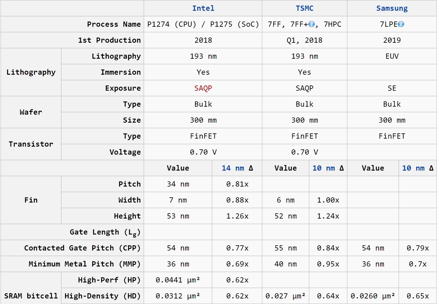
The delta 14nm / delta 10nm column shows how much each Company has shrunk a particular feature compared to the previous node. Intel and Samsung have a stricter minimum metal range compared to TSMC. But TSMC’s high-density SRAM cells are smaller than Intel’s, likely reflecting the needs of different customers at the Taiwanese foundry.
On the other hand, Samsung’s cells are even smaller than TSMC’s. However, in general, Intel’s 10nm process has the same basic criteria as the process that both TSMC and Samsung call 7nm.
We don’t yet know how Intel’s 7nm process will compare to the 5nm/3nm processes to be adopted by TSMC and Samsung. Intel has stated that it wants to regain overall process leadership by 5nm. At best, this fabrication technology will be released in late 2024-early 2025.
What is Chip Production Technology?
In English sources, you can see terms such as “process node”, “process technology”, “technology node” and just “node”. They all lead to the same door. The word “node” means “node”. We can use this as a “circuit node”. As you know, the transistors on the chips are extremely close to each other, on the scale of nanometers. We can define this structure as a “node” because they come one after the other. However, we generally prefer to use clearer terms such as process technology, production technology and fabrication technology.
Process node refers to a specific semiconductor manufacturing process and the design rules of this process. Nodes in ip production include interconnection range, transistor density, Type and other It shows the features that the production line can create on an integrated circuit, such as new technologies.

The production techniques called 5nm and 7nm are related to the “chip production” processes that take place in production facilities, which we also call foundries. Although almost all chips are produced using silicon, there are different manufacturing processes that foundries can use. That’s why we use the word “process”. In summary, when producing silicon chips, the size of the transistor components is measured, and with these dimensions, “special” production methods emerge.
Processors consist of many transistors, expressed in billions, and the more transistors inside a processor, the better. So how can we get so much performance by placing unlimited transistors? Unfortunately, goals in the world of technology do not progress in this direction. We can call the concept of “miniaturization” in the design and advancement of integrated circuits. Giants, which have been in the foundry business for years, continue to reduce the transistor range relentlessly. Process technologies are being developed with the aim of endlessly “making smaller”.
If a large number of transistors were placed without miniaturizing the process technologies, we would be using huge processors reaching gigantic sizes. Thus, heat production would increase greatly and we could not use small technological devices. Technology Companies strive to pack more transistors on a chip by reducing the gap between transistors to increase density. As newer and better processes are invented, transistor density increases, efficiency increases, space becomes smaller, and we can achieve performance without the need for large chips.
The different processes or nodes are separated by a length historically measured in micrometers and nanometers. As we mentioned, the higher the density and the lower the number, the better. In the past, the number before the phrase “nm” was used to express the physical dimensions of a transistor that manufacturers wanted to shrink when creating a new process. However, after 28nm, this figure did not have much importance. Of course, it is still important, but not like before.
The 5nm (N5) technique of TSMC, one of the largest foundries, is actually not exactly “5nm”. TSMC just wants you to know that it is better than 7nm and not as good as 3nm. For the same reason, this figure cannot be used to compare modern processes; TSMC’s 5nm process is completely different from Samsung’s 5nm. Intel, on the other hand, had to decide on a completely different nomenclature. Another example is TSMC’s 4nm (N4) technology. In fact, N4 is considered a part of the 5nm (N5) family. To make it more understandable, we can express it as improved 5nm.
New processes not only increase density, but also increase clock speed and efficiency. For example, TSCM’s 5nm technique (which you see in the Ryzen 7000 and RX 7000 series) offers 15% higher clock speeds at the same power compared to the old 7nm process ı or % at the same clock speed It can provide 30 lower power. Manufacturers can also make improvements using a combination of the two depending on their needs.
Now let’s briefly explain transistors, and then continue our topic.
What is Transistor?
Let’s open a parenthesis here and talk about transistors. A transistor is a miniature device that regulates or controls the flow of current or voltage, as well as amplifying, generating, and acting as a switch/gateway for these electrical signals. It is semiconductor. Typically transistors consist of three layers, or terminals, made of semiconductor material, each of which can carry a current.
When operating as an amplifier, the transistor converts a small input current into a larger output current. species. As a switch, it can be in one of two different states (on or off) to control the flow of electronic signals through an electrical circuit or electronic device.
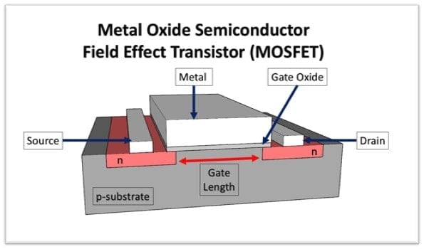
Large numbers of transistors are used to create microprocessors in which millions of transistors are placed into a single integrated circuit. It is also used for MP3 players, smartphones, cameras, memory chips and storage devices. Transistors are embedded deeply within all integrated circuits that are part of every electronic device. There can be billions of transistors inside a chip.
In summary, when silicon chips are produced, the size of the transistor components is measured, and with these dimensions, “special” production methods emerge. We can say that the most important factor in the design and progress of integrated circuits is “miniaturization”. Giants, which have been in the foundry business for years, continue to reduce the transistor range relentlessly. Process technologies are being developed with the aim of endlessly “making smaller”.
As the transistors become smaller, electrical signals pass between these transistors faster. Thus, while energy consumption decreases, performance increases proportionally. “Placing more transistors in tighter spaces” means “more computing power per square inch”.
Now let’s continue. We can say that the driving force behind process scaling is Moore’s Law. According to this law, which determines the target of rope production technologies, in order to double the density, the contacting poly pitch (CPP) and the minimum metal gap are required. (MMP) needs to be scaled roughly 0.7x at each node. In other words, 0.7x CPP â‹… 0.7x MMP ≈ ½ field scaling. We will talk about Moore’s Law in more detail shortly.
Not All New Chips Use Advanced Technologies
Current technologies, in other words small-sized transistors, are found in advanced CPUs and SoCs. However, 8-bit and 16-bit microcontrollers (MCUs) are used by billions of people every year and are used in different types of devices. As we mentioned, some devices may contain many chips with a very simple structure. In fact, the cost of some chips can drop as low as 0.5 dollars. Such chips need much fewer transistors.
The Role of Nanometers in Performance
There are many factors that affect the performance of a semiconductor circuit. These transistor properties, expressed in nanometers, are one of the factors that show whether a chip is powerful or not. Is it important? Yes, but not everything depends on this.
A new process could reduce chip sizes, increase clock speeds, and make the chip more efficient without making major changes to the design or architecture. These are all very important issues. On the other hand, there are different factors such as packaging technologies, software-side optimizations and artificial intelligence.
Additionally, it is not possible to predict the proficiency of a chip based on its process alone. As we just mentioned, for example, Intel’s 10nm technology is as good as TSMC’s 7nm. Moreover, foundry technologies are not the only thing important in an integrated circuit.
Long story short, the processing node of a chip does not mean anything by itself. To make an analogy, you cannot buy a CPU just by looking at the number of cores. Likewise, production technologies and the company that produces them do not mean anything on their own.
Which Companies Are Involved?
The number of companies using pioneering production technologies such as 5nm, 7nm and 10nm is quite low: TSMC Taiwan Semiconductor Manufacturing Company, Samsung and Intel. This trio also produces in all new and old processes. When we switch to 14/16nm processes, names such as UMC, SMIC and GF (GlobalFoundries) are added to the list.
20/22nm chip production is done by GlobalFoundries, Samsung, TSMC and Intel. As we move towards larger transistors, the number of companies is increasing. For example, companies advancing with 28/32nm fabrication technology include names such as Panasonic, STM, HLMC, IBM, UMC and SMIC.
When we go to 40/45nm, 65nm and 90nm, the number of companies producing is gradually increasing. When we come to 180nm, the number of companies producing it increases to 30. Let’s take a brief look at the historical developments:
- In 1997, 250nm technique was used.
- 180nm technologies were used by companies such as Intel, Texas Instruments, IBM and TSMC since 1999.
- Just 2 years later, Intel, Texas Instruments, IBM and TSMC introduced 130nm processes.
- The 90nm technique was introduced in 2004 by AMD, Infineon, Texas Instruments, IBM and TSMC.
- In 2006, names such as Intel, AMD, IBM, UMC, Chartered and TSMC switched to 65nm technologies.
- Matsushita, Intel, AMD, IBM, Infineon, Samsung, SMIC and Chartered Semiconductor stepped into 45nm.
- The first 14nm scale chips were shipped to consumers by Intel in 2014.
- Samsung first introduced 10nm chips in 2017.
- TSMC announced 7nm technologies in 2017, production started in 2018.
What is Moore’s Law?
Moore’s Law, first written in 1965, stated that the number of transistors on an integrated circuit would double every year. This law played a guiding role in constantly moving the semiconductor industry forward. In 1975, Moore revised this law, predicting that transistors would double in size every two years. Despite much controversy and some setbacks, Moore’s Law has largely remained valid.
On the other hand, this law says that we can expect the speed and capacity of our computers to increase every two years, but we will pay less for technological devices. Another principle of Moore’s Law suggests that this growth is exponential.
Let’s go into a little more detail. Gordon E. Moore, one of the founders of Intel, said that the number of transistors that can be packed into a given unit area doubles approximately every two years. He claimed that he was escaping. Gordon Moore did not actually name his observation “Moore’s Law” or set out to create a “law”. Moore made this statement after noticing trends in chip production at Fairchild Semiconductor. Eventually, Moore’s prediction turned into a prediction, which became the golden rule known as Moore’s Law.

Following Gordon Moore’s personal observation, Moore’s Law has guided the semiconductor industry in long-term planning as well as goal setting for research and development (R&D). From another perspective, this law reflects the technological and social change, productivity and economic change that marked the late 20th and early 21st centuries. driving growth It has had power.
In fact, this law guided by Moore is quite positive for us, the end consumers. We all always expect faster technological devices and affordable prices. Moore’s Law says that computers, computer-powered machines, and computing power become smaller, faster, and cheaper over time as transistors in integrated circuits become more efficient. So, even after more than 60 years, we still feel the lasting impact and benefits of Moore’s Law in many ways.