
Semiconductor production is a very complex process carried out to create integrated circuits (IC) used in electronic devices. All modern technological devices, from smartphones to computers, from cars to medical devices, contain one or more chips. So how are these chips produced? Our topic today is disk-shaped wafers, the images of which you constantly encounter on the internet, and which attract the attention of technology enthusiasts. Silicone plate or silicone disc plates as they are called in Turkish. We will also take a closer look at chip production processes.
Semiconductors have higher electrical conductivity than insulators, but lower than pure conductors. Silicon stands out as the most important semiconductor material used in the production of semiconductor components. Rope production is a long process that includes many steps. Silicon wafers, which we call wafers, represent the final state of the “chips” before they appear. Let’s go into details..
What is Silicone?
Silicon, an important semiconductor, is an indispensable part of the technology sector due to its conductivity and accessibility. Silicon is the second most abundant element on earth in terms of abundance. Common silicon-containing materials include beach sand, quartz and flint. Today, silicon is produced by heating sand (SiO2) together with carbon to temperatures approaching 2200°C.
Although silicon crystals resemble metals, they are not real metals. Pure silicon crystals act as insulators, allowing minimal electrical flow, but this can change through processes called doping. The electrical properties of semiconductors are regulated by a process known as doping. With this process, the entry of foreign substances is allowed in a controlled manner, and the purity of the substance is changed. Small amounts of other elements can be added to the semiconductor material, creating an excess or deficiency of electrons.
In other words, doping is a method adopted to change the behavior of the material and integrate it into a conductor. It can be defined as the process of mixing a small amount of impurities into a silicon crystal. These impurities used for doping are called dopant. Silicon (Si) by itself does not conduct electricity very well; but it can take exactly the dopants to control the resistance to a precise specification. Resistance, measured in ohm-centimeters (ohm-cm or Ω⋅cm), measures how effectively the material conducts or resists electric current. Silicon (Si) dopants such as nitrogen, indium, aluminum, gallium and boron can be added during the growth process. In order to create a semiconductor from non-conductive silicon, the aim is to turn the silicon into a wafer. After countless processes are carried out in laboratories where even small dust particles are important, cylindrical disk plates emerge.
What is Semiconductor Chip?
In semiconductor manufacturing, the chip is also known as an integrated circuit (IC). Tiny electronic devices made of semiconductor material are resistors, transistors, capacitors, etc. It is a set of electronic circuits containing a compact assembly of interconnected components such as These components are etched onto the chip, which consists of semiconductor material such as silicon or germanium.
Electronic circuits on the string are created by depositing layers of different materials and etching patterns into them. The result is a complex electronic circuit network consisting of interconnected components that can perform various functions.
Strings are characterized by their size, structure and functionality. The size of a chip is typically measured in millimeters and can vary depending on the complexity of the circuits it contains. For example, a simple logic chip might be just a few millimeters across each side, while a complex microprocessor might be 20 mm or more across each side.
The structure of a chip refers to the arrangement of the components it contains: such as the layout of circuits and the placement of transistors, resistors and capacitors. The design process is very important to optimize performance and reduce power consumption. Engineers spend long periods of time and companies spend large amounts of money in the design process.
The functionality of chips depends on the circuits they contain. While some chips, such as memory chips, have a single function, microprocessors are multifunctional. Functionality is determined by the design of the circuits and the way they are connected to each other.
Now we will take a closer look at the production process of both silicon disk wafers and chips.
What is Wafer?
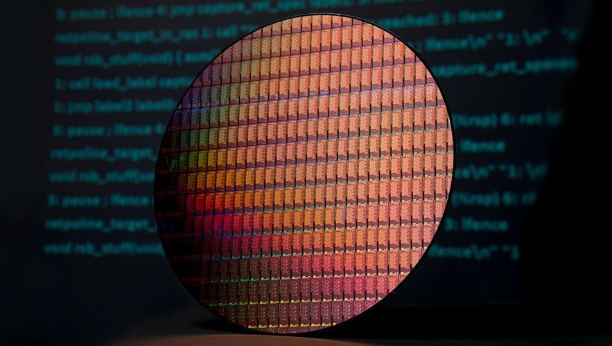
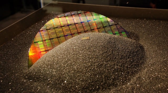
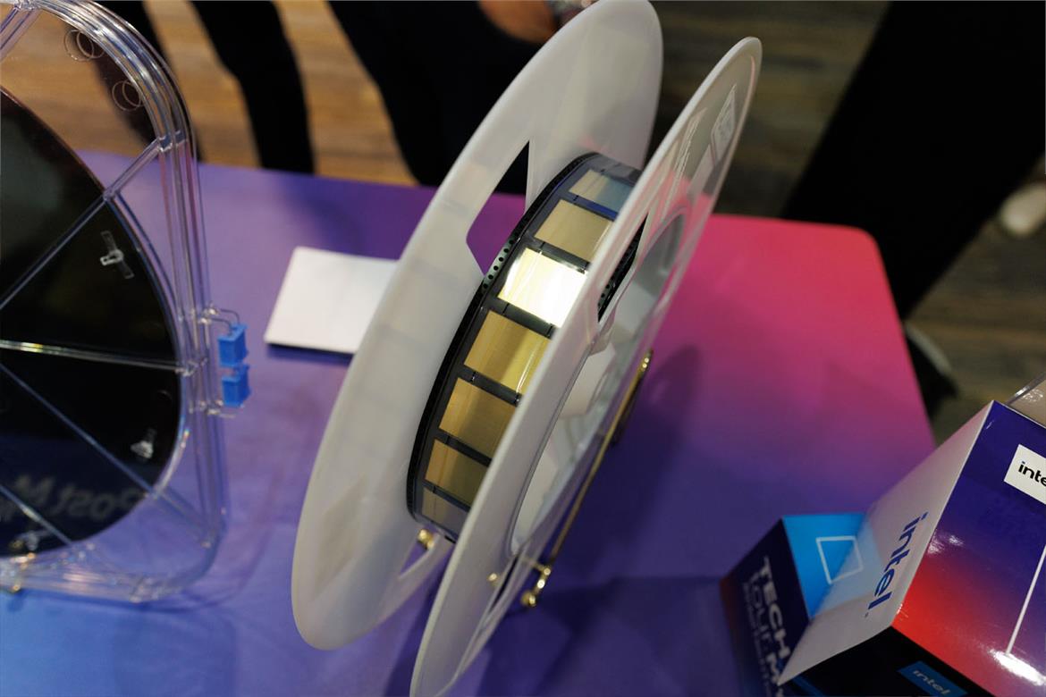
wafer Silicon disk wafers, known as wafers, are a key component in the technology industry that serves as substrate material for microelectronic devices. Microelectronic products such as integrated circuits and microchips are made by cutting them from wafers. The thin semiconductor layer forms the basis of integrated circuits used in countless technological products. Typically wafers are circular in shape and often very thin.
Available in various shapes and sizes, silicon wafers are an integral part of integrated circuits that play a vital role in electronic devices. Silicon wafers undergo manufacturing methods such as Vertical Bridgeman, Czochralski tensile and the newly emerging Float Zone, which are known for fewer defects and superior purity.
Silicon wafer production is a complex and delicate process. Essentially, during this process, raw silicon is transformed into an extremely pure, single-crystal substrate. Additionally, the process requires advanced technology and strict quality control to meet the exacting standards of the technology industry and ensure the production of high-quality wafers.
Miniaturization of electronic components, made possible by the use of silicon wafers, has allowed the development of increasingly compact and powerful devices. So we can say that semiconductor production has played a major role in the change of the world from the beginning to the end. Silicone plates are one of the most basic parts of this work.
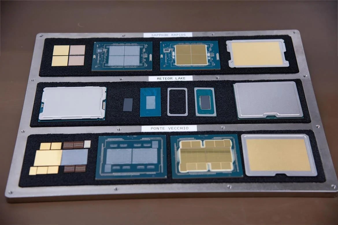
Whether it’s a standard CPU, a dedicated graphics processor, or DRAM used as system memory, all chips are made of ultra-pure silicon disks layered with metals, insulators, and semiconductor materials. r. High-quality devices are needed to realize the ultra-precise plans of the engineers who designed to obtain a final chip, down to the finest detail. Leading semiconductor giants such as TSMC, Intel and GlobalFoundries produce millions of wafers every year.
Factories even take into account bacteria and dust particles in the air to keep production near perfection. In order not to be affected by such negative things, production areas are slightly pressurized. Workers in semiconductor facilities wear protective clothing to prevent skin cells and hair from entering the machines.
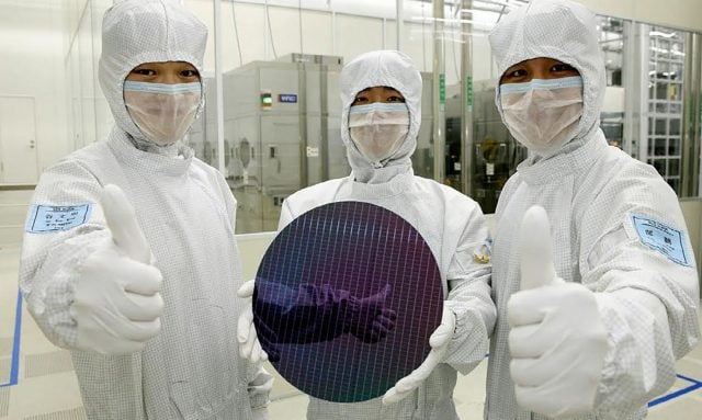
A wafer whose production has been completed looks like the one above. Each of these very valuable disk platters costs thousands of dollars, and the entire production process, from the silicone slab to the final product, takes months from start to finish. Chips cut from the disk are used in units such as CPU and GPU. Therefore, it is important to evaluate each chip in order to recover the money spent on the wafer obtained.
Chips, which generally have a rectangular structure, are cut from the wafer with the help of a diamond saw. There is something that many people wonder about. Since the chips on the edge of the round plate cannot be completed, some of them become waste, so to speak. Depending on the current situation, 5 to 25% of the silicon plate is lost. ™i (this amount varies depending on the size of the chip) is thrown away. The remaining parts are then mounted on the circuit board, usually covered with an integrated heat spreader (IHS). So, we are talking about the outer surface of the processor you install on your motherboard.
Wafer Diameter and Thickness
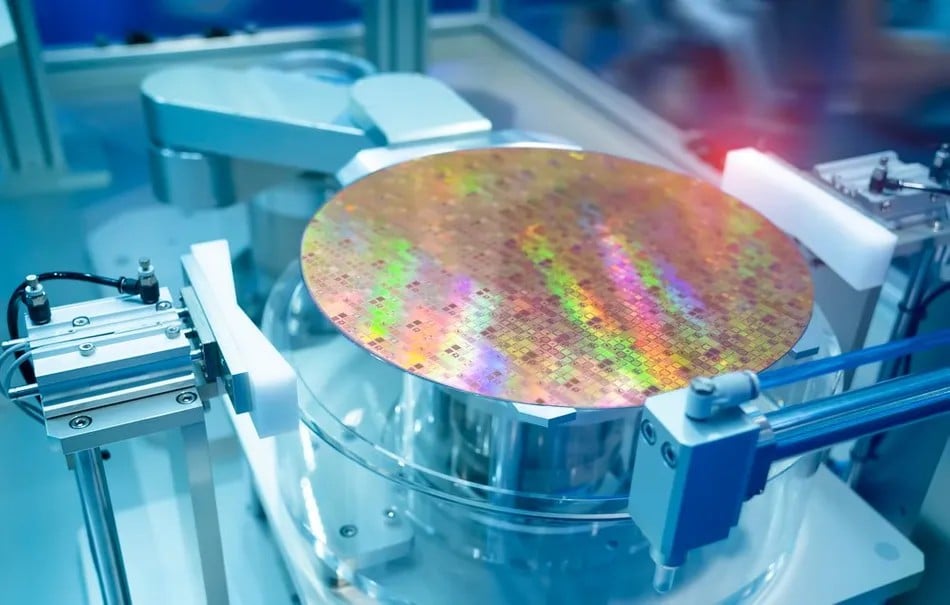
Disc plates are characterized by their diameter and thickness. Wafer diameter has increased steadily over the years to increase productivity and reduce cost per chip. Currently, the standard wafer diameter is 300 mm or approximately 12 inches, but production is also available in 450 mm sizes. Its thickness is generally a few hundred micrometers.
The surface of the wafer is polished like a mirror surface to remove defects that may affect the performance of microelectronic devices built on it. Additionally, the wafer must be extremely flat to ensure suitable photolithography later.
Quality and Purity
The silicon used in making wafers must be 99.9999% pure, which is a purity level known as “six nines”. Otherwise, impurities may prevent devices built on the wafer from functioning.
Materials Used
Plate type and materials can vary greatly depending on the type of semiconductor device that needs to be fabricated. The following materials are used for semiconductor production:
- Silicon Germanium (SiGe)
- Sapphire (Al2O3)
- Gallium Arsenide (GaAs)
- Gallium Nitride (GaN)
- Diamond
- Zinc Oxide (ZnO)
- Silicon Carbide (SiC)
- Indium Phosphide (InP)
How are silicone plates from which the threads are cut produced?
Wafer manufacturing goes through a multi-step path that begins with the extraction of raw silicon from quartz. Although silicon (Si) is the second most abundant element on Earth, it is not found in pure form. Instead, it typically exists in the form of silicon dioxide (SiO2) or quartz. During the extraction process, the quartz is heated in a high-temperature furnace in the presence of carbon, thus reducing silicon dioxide to silicon.
After the raw silicon is extracted, it must be purified to a high degree. So why? The performance of electronic devices is extremely sensitive to impurities in the silicon substrate. The purification process involves various processes that collectively increase the purity of silicon to a level of 99.9999% or higher, including purification, zone melting, and solidification. Ä Contains comments. It is then allowed to solidify into a silicon rod or ingot using common manufacturing methods such as the Floating Zone or Czochralski process. In the Czochralski method, a small piece of solid silicon is placed in a pool of molten silicon, then slowly falls as the liquid turns into a cylindrical nugget. It is pulled down by being put down.
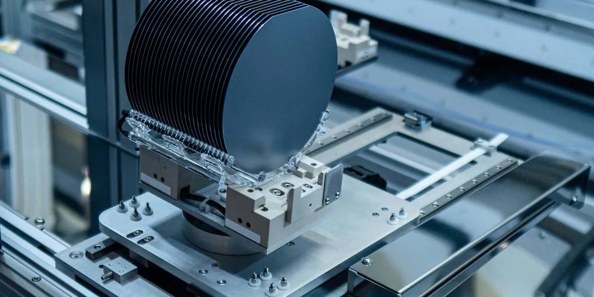
This is why the wafer is disk-shaped. The pyramidal ends of the ingot are pulled off before it cools completely. Sharp diamond saw blades are then used to slice the body into thin wafers of uniform thickness. The discs are typically around 1 millimeter thick, but can be made slightly thinner upon request. After slicing, the wafers are polished to create a smooth, flat surface suitable for manufacturing electronic devices.
What Exactly is the Czochralski Process?
The Czochralski process is a crystal growth method used to obtain single crystals of semiconductors, metals, salts and synthetic gemstones. This method, named after the Polish scientist Jan Czochralski, who invented it in 1916, is used to produce single crystal silicon used in semiconductor devices. The process begins by dipping a seed crystal into a crucible containing molten silicon. As we just mentioned, the seed crystal attached to a stick is slowly pulled up and rotated at the same time.
As the seed crystal is removed, the molten silicon cools and solidifies, preserving the crystal structure of the seed. The seed crystal removal rate and the temperature of the environment are carefully controlled to ensure a homogeneous crystal structure. The result is a large, cylindrical silicon crystal known as a “boule”. The Czochralski technique is renowned for producing high-quality crystals with few defects and is the primary method of choice for producing silicon wafers in the semiconductor industry.
Wafer Slicing and Polishing
After creating the “boule” with the Czochralski process, the next step is slicing and polishing. Boule, a single cylindrical silicon crystal, is sliced into thin discs using a diamond saw. Diamond saw is preferred due to its high hardness, which allows precise and clean cutting. The slicing process must also be carefully controlled to ensure that the sheets are of equal thickness and free of defects. Any irregularities in the wafer can affect the performance of the semiconductor devices they are used to manufacture. So the slicing process is a critical step in silicone production.
After the boards are sliced, they go through a series of cleaning and polishing steps to prepare them for the production of electronic devices. In the first step, the cleaning process is carried out to remove the silicon dust remaining from the slicing process. This process is typically done using a combination of chemicals and ultrasonic agitation. The thin plates are then polished to create a smooth, flat surface.
As for the polishing process, “polishing slurry” is used here, which is a mixture of chemicals and abrasive particles. To ensure a smooth surface to mak For this purpose, both sides of the plate are polished carefully. This is very fine workmanship.
The polishing process not only improves the physical appearance of the wafer, but also improves its electrical properties. During the fabrication of semiconductor devices, a smooth, flat surface is required for the subsequent deposition of thin films or layers of other materials. As a matter of fact, slicing and polishing processes are the most and critical steps of high quality silicon wafer production.
First Films on Sheets
We can briefly define thin films as the material layer or coating deposited on the wafer surface. These thin layers can serve various purposes and are crucial for the fabrication of semiconductor devices. Deposition of films is another important step in the manufacturing process and a layer of material is applied onto the wafer to achieve certain properties/functions. Here are a few common types of thin films used in silicon disk wafer technology: Dielectric thin films, metal thin films, semiconductor thin films, and passivation films.
Deposition of these thin films is typically done using techniques such as chemical vapor deposition (CVD), physical vapor deposition (PVD), or atomic layer deposition (ALD). The choice of thin film materials and deposition methods depends on the specific requirements of the semiconductor device being manufactured.
Cleaning Phase
The final step in the wafer building process is cleaning. The carefully produced plates that we have been talking about for a while are cleaned to remove any residual particles or contaminating substances that could hinder the production process. This process is done using a series of chemical baths and rinse cycles.
Tests Are Next
After all production stages, the wafer goes through a series of processes to create seamless integrated circuits. Oxidation and photolithography are two of the processes; Here a pattern of the integrated circuit is transferred onto the wafer using light. Then, the patterned wafer goes through some processes as follows:
- Etching
- Doping
- Test
After the silicone part is tested, it is cut into individual chips, which are packaged and prepared for use in electronic devices.
Parts of Silicone Disc Plate
Now we can look at the components of a sheet that is ready for use.
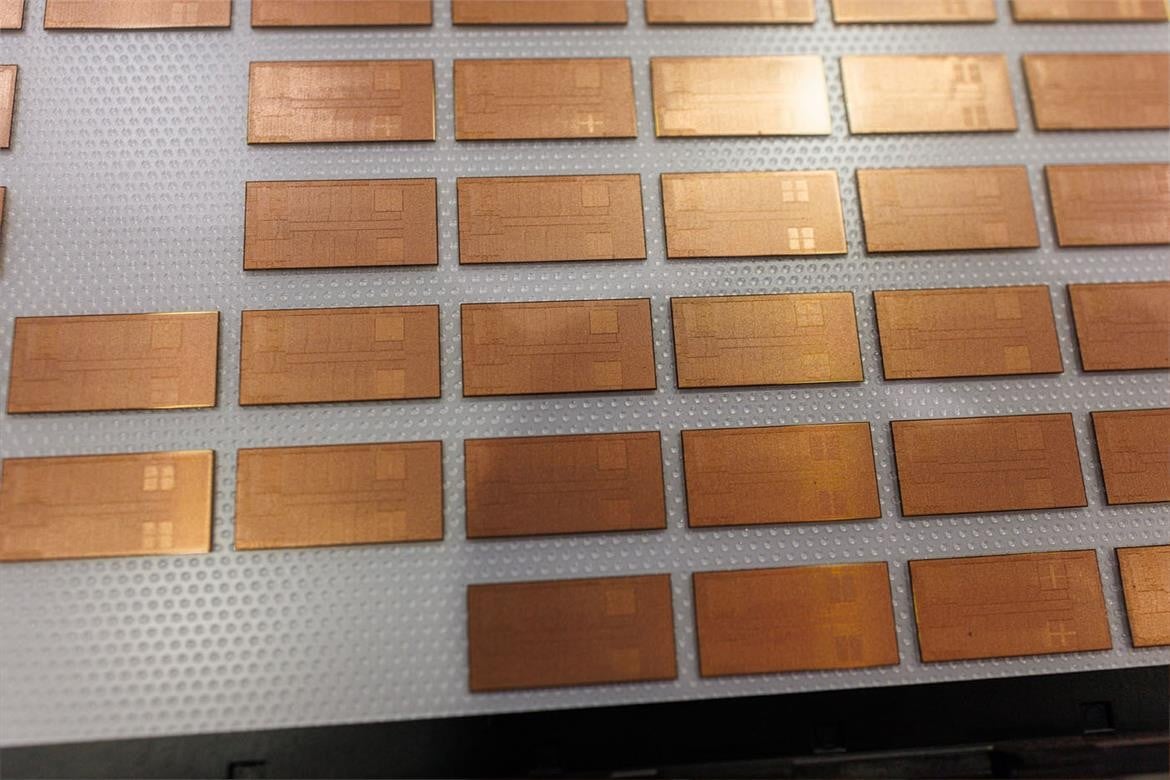
- Edge Mold (Chips): It is considered as production loss. These are chips located along the edge of a wafer. There is less chip loss in larger wafers.
- Drawing Lines: Between the functional parts there are narrow, non-functional areas where a saw can safely cut the wafer without destroying the circuits. These thin areas are known as “scribe lines”.
- chip: Silicone parts with electronic circuit patterns, for which billions of dollars and time were spent.
- Flat Region: Wafer edge pulled flat to aid wafer orientation and type identification.
- Test Element Group (TEG): A prototype model that shows the actual physical properties of a chip (diodes, circuits, capacitors, transistors, and resistors). This way it can be tested to see if it is working adequately.
How to Build a Chip?
The chips cut from wafers then go through different processes. Chip production involves various steps, including photolithography, etching and doping, which are repeated many times to create the complex structures of the chip.
Photolithography
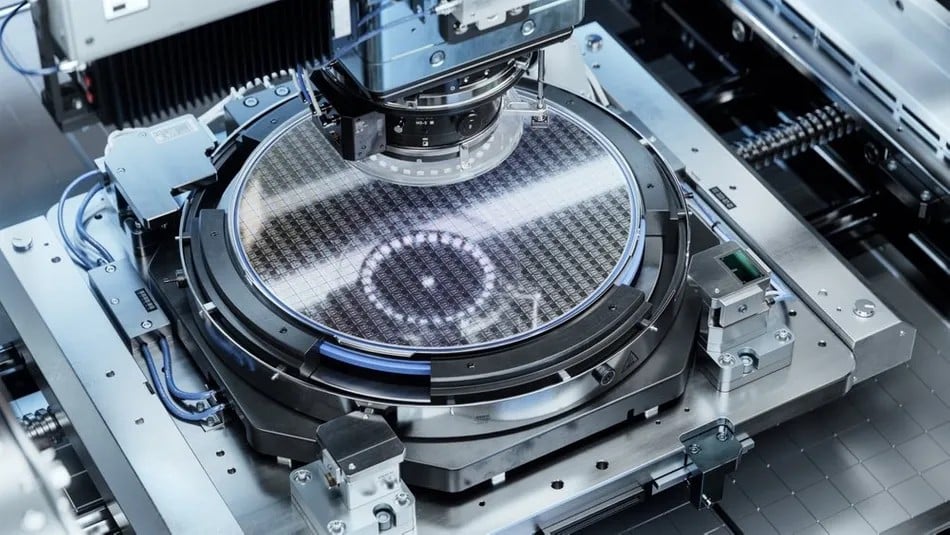
Photolithography, in its simplest terms, is the process of transferring the circuit design onto the wafer. During this process, the wafer is coated with a light-sensitive material called photoresist. The mask, a template of the circuit design, is then placed on the wafer and ultraviolet light is shined on it. The light hardens the photoresist in the pattern of the circuit design, while unexposed areas remain soft.
Etching (Etching)
In a process called etching, exposed areas of the wafer are worn away to create the features of the chip, and unwanted material is removed using chemicals that leave the desired pattern behind. It is eliminated. In addition, in this process, the silicon and other material layers underneath the circuit design are also eliminated.
Doping
We actually explained it in detail a while ago, let’s go over it again with a different explanation. Doping is a technique used to change the properties of the silicon inside the disk to create different components of the chip. This process is done by adding impurities to silicon that change its conductivity. The type and amount of impurities determine whether the silicon will be n-type with excess electrons or p-type with electron deficiency. The interaction between n-type and p-type silicon forms the basis of the transistors that form the circuits on the chip.
Photolithography, etching and doping processes can be repeated many times to create complex structures of the chip. Each iteration adds a new layer to the chip, and each layer serves a specific function in the final circuit.
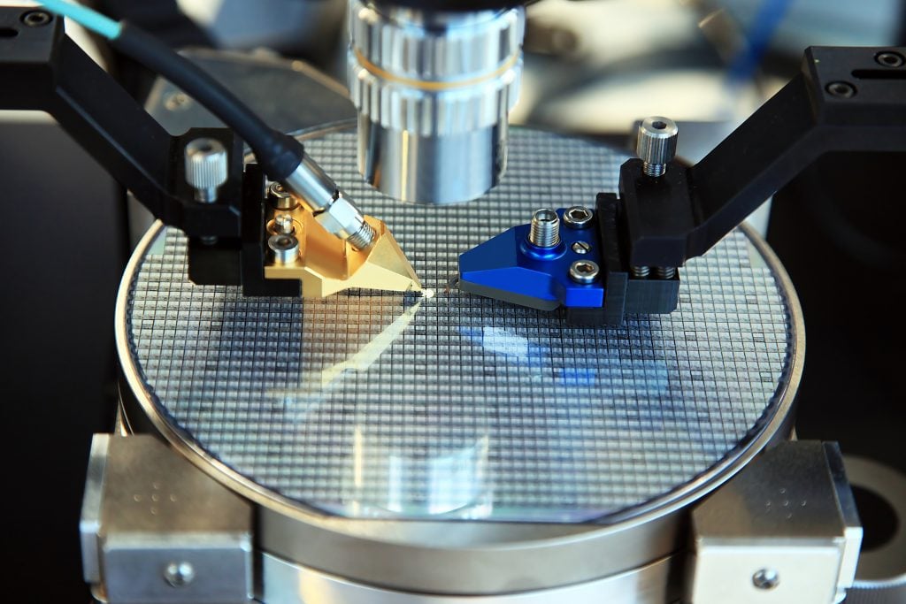
Functionality Testing
Independent of wafer testing, the chip is tested for functionality and performance after it is created. At this stage, electrical signals are applied to the chip and its response is tested. If the chip passes the tests, it is cut from the chipboard and packaged to be used in electronic devices.
Packaging Process of Chips
If you remember, we had the opportunity to visit Intel’s chip packaging factory in Malaysia in 2023.
Intel is one of the few companies involved in every stage of chip production. The stages are turning sand into silicon chips (by a partner company) and then etching the design using the latest lithography process (varies from chip to chip). It starts with getting it. Once the etching process is completed, these 300 mm (typical circular wafer size) wafers are rolled from manufacturing facilities to die preparation and grading operation facilities such as the one in Kulim, Malaysia. being sent.
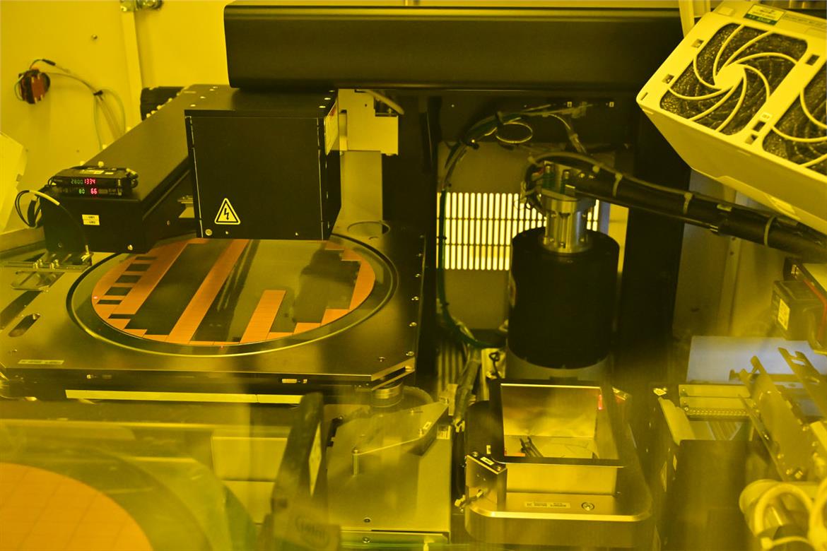
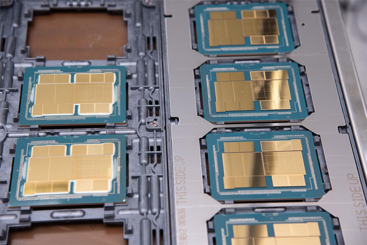
The mold is then separated into individual chips using various methods such as grinding, laser engraving and mechanical cutting. These chips are placed in a transmission mechanism, checked for defects and sorted using a special in-house module weighing more than 450 kilograms . Additionally, the entire process takes place automatically.
Now let’s go into more detail. Mold separation is a multi-step process. First of all, the chip sections are pre-marked with lasers. Then, another machine comes into play, which literally separates the chips with a saw, in a process called singulation. This machine is supported by two diamond tipped blades to increase efficiency. The blades cut cleanly through the plate, while a stream of cooled water runs through it to both help remove debris and prevent thermal expansion from damaging the sensitive chips. The system comes into play. The entire chip cutting system monitors factors such as blade integrity in detail to ensure cuts remain clean and precise.
A different machine takes the separated individual chips, then systematically removes each die onto a tray called a Pick & Place. tiring. The robotic arm then guides each mold to a designated position on the tray.
Intel says these trays are used effectively in all its products. There are no sockets to place the chips. Instead, a white material perforated with a hexagonal grid of holes was used on the bed of the tray. Apparently, the material provides a slight suction pressure when inserting the chips, which allows the trays containing the chips to be carried through the facilities without shaking.
Testing and Classification
Intel tests the dies individually using a machine the size of a bus. One section contains twenty test cells, each weighing approximately 450 kg. These are approximately 1.5 meters wide, 1.5 meters deep and 1 meter high. Lots are loaded from one end, then a robotic system in the center dispenses chip trays to the available test cells, similar to a giant vending machine. Each test cell takes a tray, then automatically processes the chips placed on the tray to test and characterize each one.
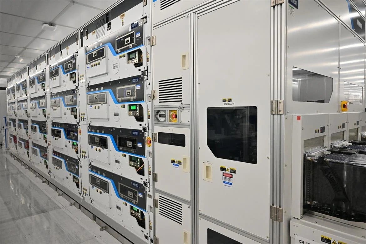
The test cells operate independently, so any unit can test different products. In fact, each of them can be disabled separately when maintenance is required. There is also a large hoist that Intel uses to move these cells around the facility as needed. This mechanism moves on an air cushion located just above the ground so that nothing is damaged. The company covered most of the floor with a plastic sheet to provide better insulation. This prevents the weight of the test cell and the apparatus from damaging the ground and also ensures maneuverability.
Testing processes are effectively carried out autonomously. Stations have been set up where an employee can monitor several rows of test devices at the same time. Employees can practically follow a large number of test devices on more than one screen. Machines do almost everything except monitoring and maintenance. So, we can say that there is no need for much human power, at least in the classification and testing steps.
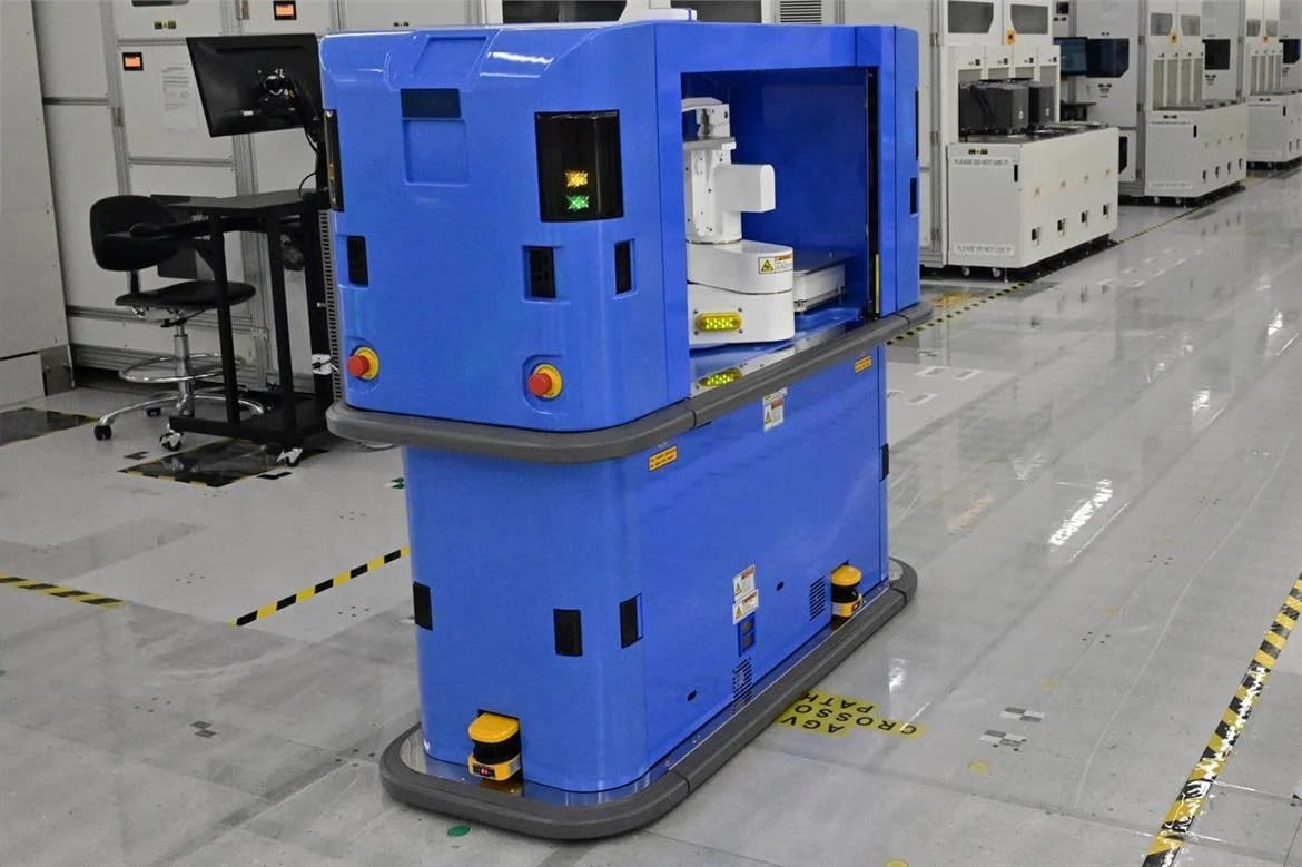
The separated chips (i.e. chip batches) are mixed between the test equipment and surrounding storage areas by automated guidance vehicles (AGV). ±yor. The system is constantly evaluating what test cells are available and where to select batches with the highest yield potential, rather than testing on a first-in, first-out basis. Vehicles called AGVs move independently on roads that do not have a specific route.
The tested trays return to a winding machine (like a reel) next to the Pick & Place machine. At this point the chips become characterized and grouped according to a specific pattern. While the trays are sorted, a robotic arm carries each chip to different reels according to the relevant model. In addition, the rollers squeeze the chips between two layers of tape so that they do not get damaged. Molds that fail the test are set aside and collected for recycling.
Advanced Packaging Techniques and Production
From there, the reels are shipped to Intel Assembly and Test facilities around the world. One of the facilities is located in the PG8 building, known as PGAT, in Penang.
The chips are first aligned and stacked, then the integrated heat spreader (IHS) is placed in place with thermal interface material (TIM) and adhesive. Beforehand, epoxy subfilling is applied and hardened. As we mentioned before, Intel also outsources production to TSMC. The facility in Malaysia is not only limited to processors produced by the company, but also packages chips produced by other foundries such as TSMC.
The subsequent Chip Attach process begins with flip-chip packaging to place the components on a substrate. Hundreds or thousands of microscopic solder balls are placed on the surface of each chip, which mate with the next chip or substrate layer.
In the meantime, let’s talk about Foveros. Foveros, a multi-dimensional inter-chip bonding technique, allows Intel to combine chips into a single package by placing them three-dimensionally on top of each other. This technique was first used with the Lakefield series.
After bonding, small air gaps may remain between the layers. Intel applies an epoxy underfill to increase stability, ensuring stresses are distributed evenly throughout the die. As with the double saw blade during singulation, here too Intel can use two epoxy dispensing nozzles to increase efficiency. There’s no need for suction or anything else, Intel says capillary action is all that’s needed to get the material to flow. The threads are then scanned to check for voids in the epoxy filler.
The package is now ready for the integrated heat spreader (IHS) that we constantly see on processors to be installed. There is a specific TIM (Thermal Interface Material) used in each chip design. The machine spreads the thermal material around in an orderly manner. To mount the IHS, adhesive is distributed, then the IHS is placed in place and hardened to make it durable.
What is the Difference Between Wafer and Chip?
Chips and wafers are words sometimes used interchangeably in the electronics world, but they are not the same thing. Chip or integrated circuit is an electronic component, while wafer is a thin slice of silicon used for the formation of integrated circuits.
What is Chip Production Technology?
In English sources, you can see terms such as ‘process node’, ‘process technology’, ‘technology node’ and just ‘node’. They all lead to the same door. The word “Node” means “node”. We can use this as a “circuit node”. As you know, the transistors on the chips are extremely close to each other, on the scale of nanometers. Since they come one after the other, we can define this structure as “nodule”. However, we generally prefer to use clearer terms such as process technology, production technology and fabrication technology.
Process node refers to a specific semiconductor manufacturing process and the design rules of this process. Nodes in chip production include interconnection range, transistor density, istor type and Like other new technologies, it shows the features that the production line can create on an integrated circuit.

The production techniques called 5nm and 7nm are related to the “chip production” processes that take place in production facilities, which we also call foundries. Although almost all chips are produced using silicon, there are different manufacturing processes that foundries can use. That’s why we use the word “processâ€. In summary, when silicon chips are produced, the size of the transistor components is measured, and with these dimensions, ‘special’ production methods emerge.
Processors consist of many transistors, expressed in billions, and the more transistors inside a processor, the better. So how can we get so much performance by placing unlimited transistors? Unfortunately, goals in the world of technology do not progress in this direction. We can call the understanding in the design and progress of integrated circuits “miniaturization”. Giants, which have been in the foundry business for years, continue to reduce the transistor range relentlessly. Process technologies are being developed with the aim of making them infinitely smaller.
Finally, let us note that the microchips obtained are classified according to their quality. Our article on this subject is right below: